
下载
1V/div
1V/div
Time(1ms/div)
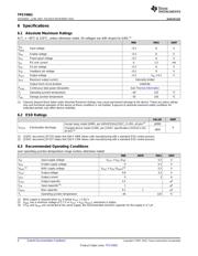
C =0 F
SS
m
C =0.001 F
SS
m
C =0.0047 F
SS
m
V
OUT
V
EN
0V
1.2V
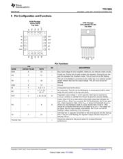
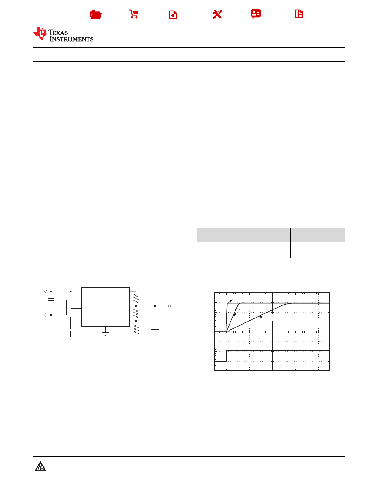
TPS74901
GND
EN
FB
IN PG
BIAS
SS
OUT
V
IN
R
1
R
2
R
3
C
OUT
C
IN
C
SS
V
BIAS
C
BIAS
V
OUT
Product
Folder
Sample &
Buy
Technical
Documents
Tools &
Software
Support &
Community
Reference
Design
TPS74901
SBVS082H –JUNE 2007–REVISED NOVEMBER 2015
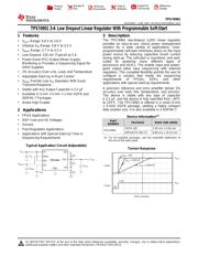
TPS74901 3-A Low Dropout Linear Regulator With Programmable Soft-Start
1 Features 3 Description
The TPS74901 low-dropout (LDO) linear regulator
1
• V
OUT
Range: 0.8 V to 3.6 V
provides an easy-to-use, robust power management
• Ultralow V
IN
Range: 0.8 V to 5.5 V
solution for a wide variety of applications. User-
• V
BIAS
Range: 2.7 V to 5.5 V
programmable soft-start minimizes stress on the input
power source by reducing capacitive inrush current
• Low Dropout: 120 mV (Typical) at 3 A
during start-up. The soft-start is monotonic and well-
• Power-Good (PG) Output Allows Supply
suited for powering many different types of
Monitoring or Provides a Sequencing Signal for
processors and ASICs. The enable input and power-
Other Supplies
good output allow easy sequencing with external
• 2% Accuracy Over Line, Load, and Temperature
regulators. This complete flexibility permits the user to
configure a solution that meets the sequencing
• Adjustable Start-Up In-Rush Control
requirements of FPGAs, DSPs, and other
• V
BIAS
Permits Low V
IN
Operation With Good
applications with special start-up requirements.
Transient Response
A precision reference and error amplifier deliver 2%
• Stable with Any Output Capacitor ≥ 2.2 µF
accuracy over load, line, temperature, and process.
• Available in 5-mm × 5-mm × 1-mm VQFN and
The device is stable with any type of capacitor
DDPAK-7 Packages
≥ 2.2 µF, and the device is fully specified from –40°C
to 125°C. The TPS74901 is offered in a small (5-mm
• Active High Enable
× 5-mm) VQFN package, yielding a highly compact
total solution size. It is also available in a DDPAK-7.
2 Applications
• FPGA Applications
Device Information
(1)
• DSP Core and I/O Voltages
PART
PACKAGE BODY SIZE (NOM)
NUMBER
• Servers
VQFN (20) 5.00 mm × 5.00 mm
• Post-Regulation Applications
TPS74901
DDPAK/TO-263 (7) 8.89 mm × 10.10 mm
• Applications with Special Start-Up Time or
(1) For all available packages, see the orderable addendum at
Sequencing Requirements
the end of the data sheet.
SPACE
Typical Application Circuit (Adjustable)
Turnon Response
1
An IMPORTANT NOTICE at the end of this data sheet addresses availability, warranty, changes, use in safety-critical applications,
intellectual property matters and other important disclaimers. PRODUCTION DATA.
页面指南