
下载
© 2009 Microchip Technology Inc. DS39687E-page 1
PIC18F2XJXX/4XJXX FAMILY
1.0 DEVICE OVERVIEW
This document includes the programming specifications
for the following devices:
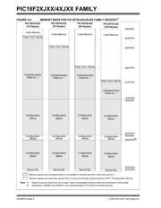
2.0 PROGRAMMING OVERVIEW
OF THE PIC18F2XJXX/4XJXX
FAMILY
The PIC18F2XJXX/4XJXX family devices are
programmed using In-Circuit Serial Programming™
(ICSP™). This programming specification applies to
devices of the PIC18F2XJXX/4XJXX family in all
package types.
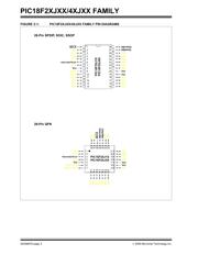
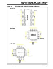
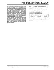
2.1 Pin Diagrams
The pin diagrams for the PIC18F2XJXX/4XJXX family
are shown in Figure 2-1 and Figure 2-2. The pins that
are required for programming are listed in Table 2-1
and shown in darker lettering in the diagrams.
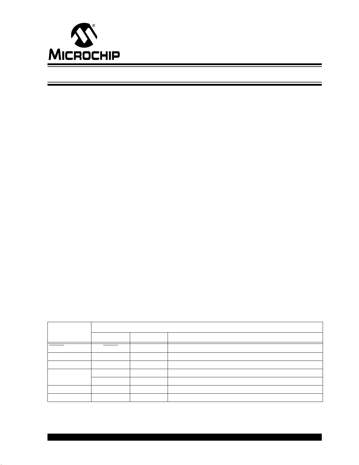
TABLE 2-1: PIN DESCRIPTIONS (DURING PROGRAMMING): PIC18F2XJXX/4XJXX FAMILY
• PIC18F24J10 • PIC18LF24J10
• PIC18F25J10 • PIC18LF25J10
• PIC18F44J10 • PIC18LF44J10
• PIC18F45J10 • PIC18LF45J10
• PIC18F24J11 • PIC18LF24J11
• PIC18F25J11 • PIC18LF25J11
• PIC18F26J11 • PIC18LF26J11
• PIC18F44J11 • PIC18LF44J11
• PIC18F45J11 • PIC18LF45J11
• PIC18F46J11 • PIC18LF46J11
• PIC18F26J13 • PIC18LF26J13
• PIC18F27J13 • PIC18LF27J13
• PIC18F46J13 • PIC18LF46J13
• PIC18F47J13 • PIC18LF47J13
• PIC18F24J50 • PIC18LF24J50
• PIC18F25J50 • PIC18LF25J50
• PIC18F26J50 • PIC18LF26J50
• PIC18F44J50 • PIC18LF44J50
• PIC18F45J50 • PIC18LF45J50
• PIC18F46J50 • PIC18LF46J50
• PIC18F26J53 • PIC18LF26J53
• PIC18F27J53 • PIC18LF27J53
• PIC18F46J53 • PIC18LF46J53
• PIC18F47J53 • PIC18LF47J53
Pin Name
During Programming
Pin Name Pin Type Pin Description
MCLR
MCLR P Programming Enable
V
DD and AVDD
(1)
VDD P Power Supply
V
SS and AVSS
(1)
VSS PGround
V
DDCORE/VCAP VDDCORE P Regulated Power Supply for Microcontroller Core
V
CAP I Filter Capacitor for On-Chip Voltage Regulator
RB6 PGC I Serial Clock
RB7 PGD I/O Serial Data
Legend: I = Input, O = Output, P = Power
Note 1: All power supply and ground pins must be connected, including analog supplies (AV
DD) and ground
(AV
SS).
Flash Microcontroller Programming Specification