
下载
SLVS171A − SEPTEMBER 1998 − REVISED MAY 1999
1
POST OFFICE BOX 655303 • DALLAS, TEXAS 75265
D ±1% Reference Over Full Operating
Temperature Range
D Synchronous Rectifier Driver for Greater
Than 90% Efficiency
D Programmable Reference Voltage Range of
1.3 V to 3.5 V
D User−Selectable Hysteretic Type Control
D Droop Compensation for Improved Load
Transient Regulation
D Adjustable Overcurrent Protection
D Programmable Softstart
D Overvoltage Protection
D Active Deadtime Control
D Power Good Output
D Internal Bootstrap Schottky Diode
D Low Supply Current . . . 3-mA Typ
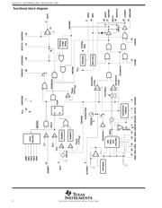
description
The TPS5210 is a synchronous-buck regulator controller which provides an accurate, programmable supply
voltage to microprocessors. An internal 5-bit DAC is used to program the reference voltage to within a range
of 1.3 V to 3.5 V. The output voltage can be set to be equal to the reference voltage or to some multiple of the
reference voltage. A hysteretic controller with user-selectable hysteresis and programmable droop
compensation is used to dramatically reduce overshoot and undershoot caused by load transients. Propagation
delay from the comparator inputs to the output drivers is less than 250 ns. Overcurrent shutdown and crossover
protection for the output drivers combine to eliminate destructive faults in the output FETs. The softstart current
source is proportional to the reference voltage, thereby eliminating variation of the softstart timing when
changes are made to the output voltage. PWRGD monitors the output voltage and pulls the open-collector
output low when the output drops 7% below the nominal output voltage. An overvoltage circuit disables the
output drivers if the output voltage rises 15% above the nominal value. The inhibit pin can be used to control
power sequencing. Inhibit and undervoltage lockout assures the 12-V supply voltage and system supply voltage
(5 V or 3.3 V) are within proper operating limits before the controller starts. Single-supply (12 V) operation is
easily accomplished using a low-current divider for the required 5-V signals. The output driver circuits include
2-A drivers with internal 8-V gate-voltage regulators. The high-side driver can be configured either as a
ground-referenced driver or as a floating bootstrap driver. The TPS5210 is available in a 28-pin SOIC package
and a 28-pin TSSOP PowerPAD package. It operates over a junction temperature range of 0°C to 125°C.
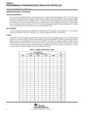
AVAILABLE OPTIONS
PACKAGES
T
J
SOIC
(DW)
TSSOP
(PWP)
0°C to 125°C TPS5210DW TPS5210PWPR
The DW package is available taped and reeled. Add R suffix to device
type (e.g., TPS5210DWR).
Copyright 1999, Texas Instruments Incorporated
! " #$%! " &$'(#! )!%*
)$#!" # ! "&%##!" &% !+% !%" %," "!$%!"
"!)) -!.* )$#! &#%""/ )%" ! %#%""(. #($)%
!%"!/ (( &%!%"*
Please be aware that an important notice concerning availability, standard warranty, and use in critical applications of
Texas Instruments semiconductor products and disclaimers thereto appears at the end of this data sheet.
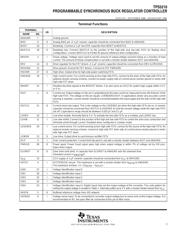
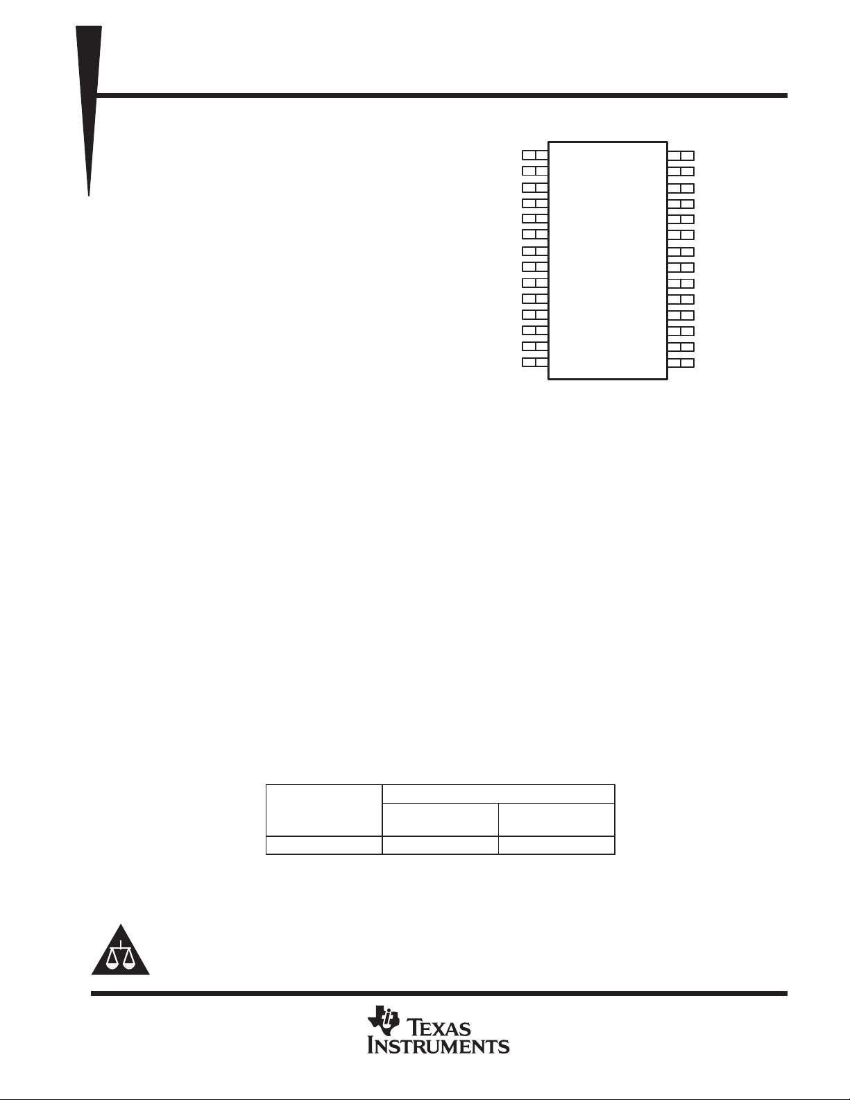
1
2
3
4
5
6
7
8
9
10
11
12
13
14
28
27
26
25
24
23
22
21
20
19
18
17
16
15
IOUT
DROOP
OCP
VHYST
VREFB
VSENSE
ANAGND
SLOWST
BIAS
LODRV
LOHIB
DRVGND
LOWDR
DRV
PWRGD
VID0
VID1
VID2
VID3
VID4
INHIBIT
IOUTLO
LOSENSE
HISENSE
BOOTLO
HIGHDR
BOOT
V
CC
DW OR PWP PACKAGE
(TOP VIEW)