
2001-2011 Microchip Technology Inc. Preliminary DS41156E-page 1
HCS365
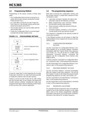
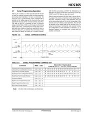
1.0 PROGRAMMING THE HCS365
HCS365 devices are programmed using a serial
method that differs from previous K
EELOQ
®
encoders.
This Serial mode will still allow the HCS365 to be pro-
grammed while in the users system (ICSP™). This
allows for great design flexibility. This programming
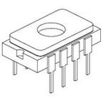
specification applies to HCS365 devices in all pack-
ages.
1.1 Hardware Requirements
The HCS365 requires one programmable power sup-
ply for V
DD (4.5V to 5.5V) and a VPP of 9V to 14V. Both
supplies should have a minimum resolution of 0.25V.
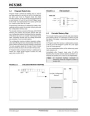
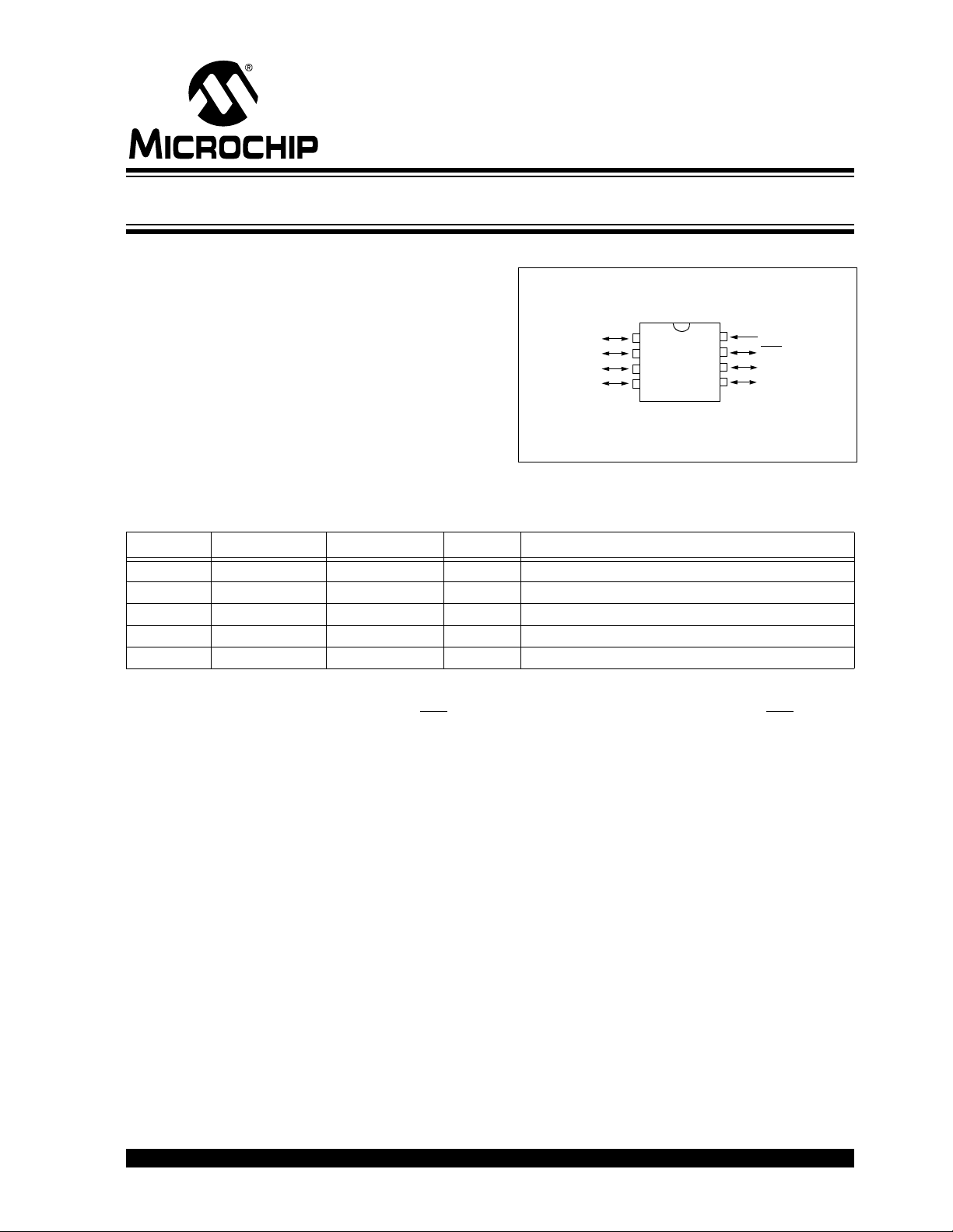
FIGURE 1-1: HCS365 DIAGRAM
TABLE 1-1: PROGRAMMING PIN DESCRIPTION
PDIP, SOIC,
HCS365
S0
S1
S2
S3
VDD
LED
OUTPUT
V
SS
1
2
3
4
8
7
6
5
Pin Name Function HCS365 Pin Type Pin Description
S0 DATA 1 I/O Data Input Output
S1 CLOCK 2 I Clock Input
LED V
PP 7 P(*) Program mode select
Vss Vss 5 P Ground
V
DD VDD 8PPower supply
Legend: I = Input, O = Output, P = Power
Note: In the HCS365, the programming high voltage is internally generated. To activate the Programming mode,
high voltage needs to be applied to LED input. This is used as a level source, meaning that LED does not
draw any significant current.
HCS365 Programming Specifications