
下载
1
FEATURES
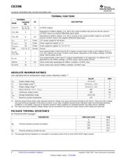
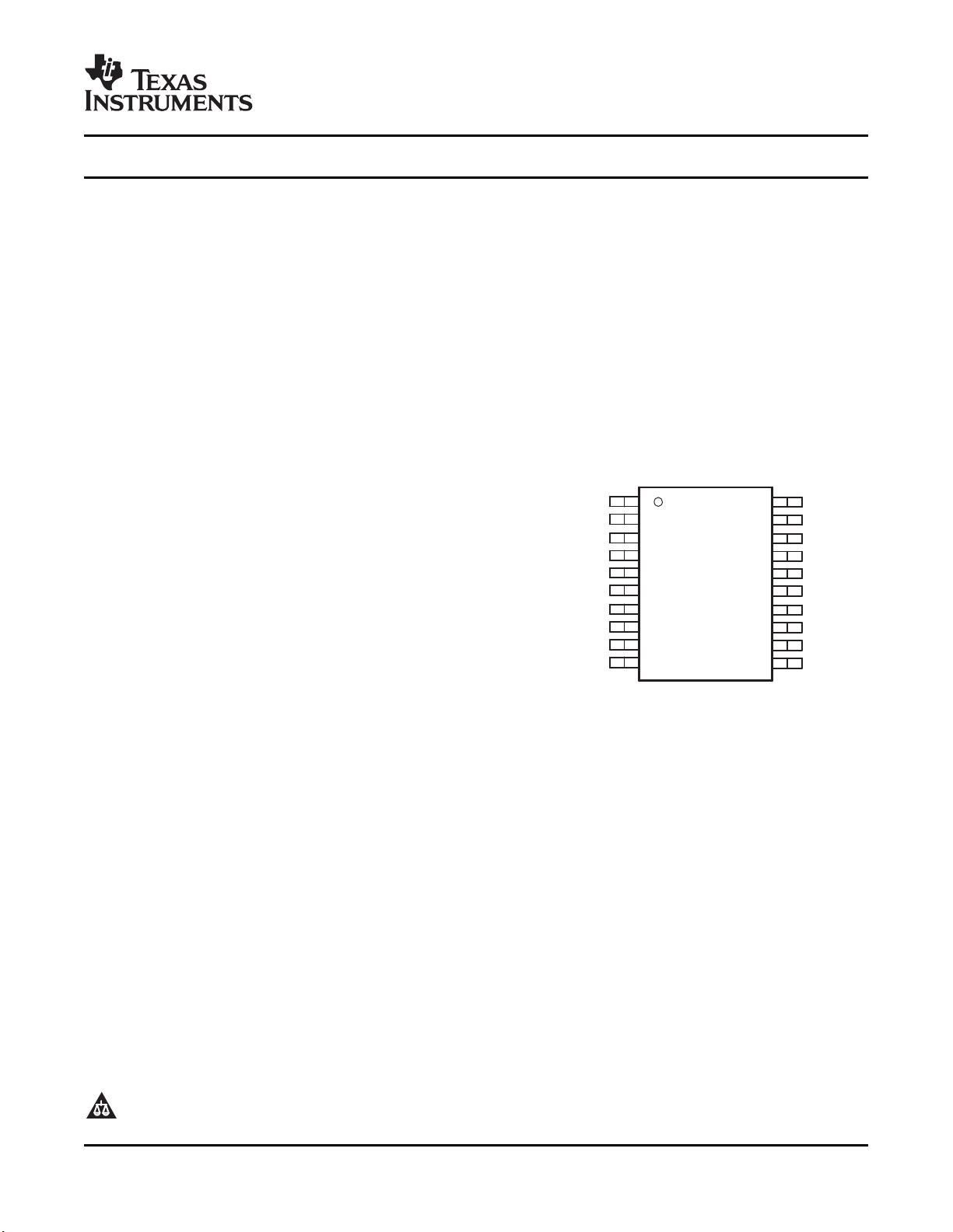
TERMINAL ASSIGNMENT
1
2
3
4
5
6
7
8
9
10
20
19
18
17
16
15
14
13
12
11
S0/A0/CLK_SEL
S1/A1
V
CC
GND
CLK_IN0
CLK_IN1
V
CC
GND
SDATA
SCLOCK
Y5
Y4
V
CCOUT2
GND
Y3
Y2
V
CCOUT1
GND
Y1
Y0
PW PACKAGE
(TOP VIEW)
TSSOP 20
Pitch 0,65 mm
6.6 x 6.6
DESCRIPTION
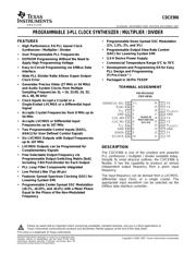
CDCE906
SCAS814H – NOVEMBER 2005 – REVISED DECEMBER 2007
www.ti.com
PROGRAMMABLE 3-PLL CLOCK SYNTHESIZER / MULTIPLIER / DIVIDER
• Programmable Down Spread SSC Modulation
(1%, 1.5%, 2%, and 3%)
2
• High Performance 3:6 PLL based Clock
Synthesizer / Multiplier / Divider • Programmable Output Slew-Rate Control
(SRC) for Lowering System EMI
• User Programmable PLL Frequencies
• 3.3-V Device Power Supply
• EEPROM Programming Without the Need to
Apply High Programming Voltage • Commercial Temperature Range 0 ° C to 70 ° C
• Easy In-Circuit Programming via SMBus Data • Development and Programming Kit for Easy
Interface PLL Design and Programming
(TI Pro-Clock™)
• Wide PLL Divider Ratio Allows 0-ppm Output
Clock Error • Packaged in 20-Pin TSSOP
• Generates Precise Video (27 MHz or 54 MHz)
and Audio System Clocks from Multiple
Sampling Frequencies (f
S
= 16, 22.05, 24, 32,
44.1, 48, 96 kHz)
• Clock Inputs Accept a Crystal or a
Single-Ended LVCMOS or a Differential Input
Signal
• Accepts Crystal Frequencies from 8 MHz up to
54 MHz
• Accepts LVCMOS or Differential Input
Frequencies up to 167 MHz
• Two Programmable Control Inputs [S0/S1,
A0/A1] for User Defined Control Signals
• Six LVCMOS Outputs with Output Frequencies
up to 167 MHz
• LVCMOS Outputs can be Programmed for
Complementary Signals
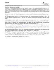
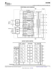
The CDCE906 is one of the smallest and powerful
• Free Selectable Output Frequency via
PLL synthesizer / multiplier / divider available today.
Programmable Output Switching Matrix [6x6]
Despite its small physical outlines, the CDCE906 is
Including 7-Bit Post-Divider for Each Output
flexible. It has the capability to produce an almost
independent output frequency from a given input
• PLL Loop Filter Components Integrated
frequency.
• Low Period Jitter (Typ 60 ps)
The input frequency can be derived from a LVCMOS,
• Features Spread Spectrum Clocking (SSC) for
differential input clock, or a single crystal. The
Lowering System EMI
appropriate input waveform can be selected via the
• Programmable Center Spread SSC Modulation
SMBus data interface controller.
( ± 0.1%, ± 0.25%, and ± 0.4%) with a Mean Phase
Equal to the Phase of the Non-Modulated
Frequency
1
Please be aware that an important notice concerning availability, standard warranty, and use in critical applications of
Texas Instruments semiconductor products and disclaimers thereto appears at the end of this data sheet.
2 Pro-Clock is a trademark of Texas Instruments.
PRODUCTION DATA information is current as of publication date.
Copyright © 2005 – 2007, Texas Instruments Incorporated
Products conform to specifications per the terms of the Texas
Instruments standard warranty. Production processing does not
necessarily include testing of all parameters.
页面指南