
下载
LVPECL 1.5GHz / LVDS 800MHz
CDCE18005
Crystal 25MHz
LVPECL 1.5GHz
LVDS 800MHz
LVDS 400MHz
LVPECL 800MHz
LVCMOS 25MHz
LVCMOS 25MHz
CDCE18005
www.ti.com
SCAS863B –NOVEMBER 2008–REVISED NOVEMBER 2012
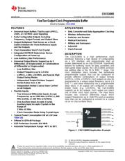
Five/Ten Output Clock Programmable Buffer
Check for Samples: CDCE18005
1
FEATURES
APPLICATIONS
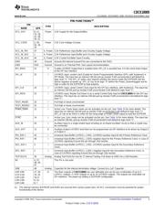
• Universal Input Buffers That Accept LVPECL, • Data Converter and Data Aggregation Clocking
LVDS, or LVCMOS Level Signaling
• Wireless Infrastructure
• Fully Configurable Outputs Including
• Switches and Routers
Frequency, Output Format, and Output Skew
• Medical Electronics
• Output Multiplexer That Serves as a Clock
• Military and Aerospace
Switch Between the Three Reference Inputs
• Industrial
and the Outputs
• Clock Fan-out
• Clock Generation Via AT-Cut Crystal
• Integrated EEPROM Determines Device
DESCRIPTION
Configuration at Power-up
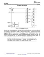
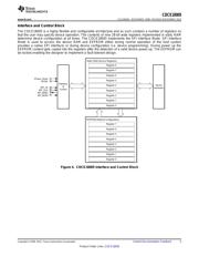
The CDCE18005 is a high performance clock
• Low Additive Jitter Performance
distributor featuring a high degree of configurability
via a SPI interface, and programmable start up
• Universal Output Blocks Support up to 5
modes determined by on-chip EEPROM. Specifically
Differential, 10 Single-ended, or Combinations
tailored for buffering clocks for data converters and
of Differential or Single-ended:
high-speed digital signals, the CDCE18005 achieves
– Low Additive Jitter
low additive jitter in the 50 fs RMS
(1)
range. The
– Output Frequency up to 1.5 GHz
clock distribution block includes five individually
programmable outputs that can be configured to
– LVPECL, LVDS, LVCMOS, and Special High
provide different combinations of output formats
Output Swing Modes
(LVPECL, LVDS, LVCMOS). Each output can also be
– Independent Output Dividers Support
programmed to a unique output frequency (up to 1.5
Divide Ratios from 1–80
GHz
(2)
) and skew relationship via a programmable
– Independent limited Coarse Skew Control
delay block. If all outputs are configured in single-
ended mode (e.g. LVCMOS), the CDCE18005
on all Outputs
supports up to ten outputs. Each output can select
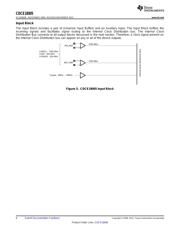
• Flexible Inputs:
one of three clock input sources. The input block
– Two Universal Differential Inputs Accept
includes two universal differential inputs which
Frequencies up to 1500 MHz (LVPECL), 800
support frequencies up to 1500 MHz and an auxiliary
MHz (LVDS), or 250 MHz (LVCMOS).
input that can be configured to connect to a crystal
via an on chip oscillator block.
– One Auxiliary Input Accepts Crystal.
Auxiliary Input Accepts Crystals in the
spacer
Range of
2 MHz–42 MHz
– Clock Generator Mode Using Crystal Input.
• Typical Power Consumption 1W at 3.3V (see
Table 28)
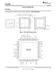
• Offered in QFN-48 Package
• ESD Protection Exceeds 2kV HBM
• Industrial Temperature Range –40°C to 85°C
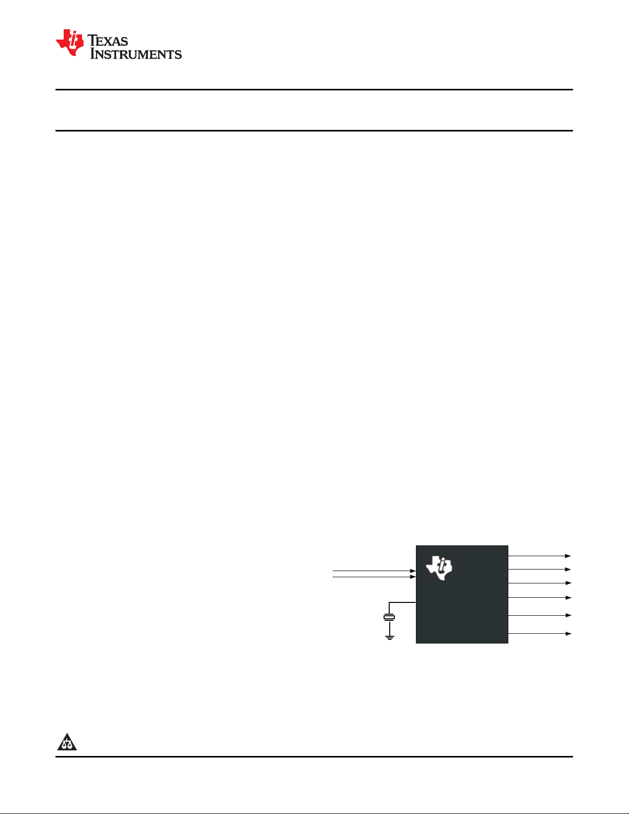
Figure 1. CDCE18005 Application Example
(1) 12 kHz to 20 MHz integration bandwidth.
(2) Maximum output frequency depends on the output format
selected
1
Please be aware that an important notice concerning availability, standard warranty, and use in critical applications of
Texas Instruments semiconductor products and disclaimers thereto appears at the end of this data sheet.
PRODUCTION DATA information is current as of publication date.
Copyright © 2008–2012, Texas Instruments Incorporated
Products conform to specifications per the terms of the Texas
Instruments standard warranty. Production processing does not
necessarily include testing of all parameters.
页面指南