

下载
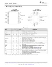
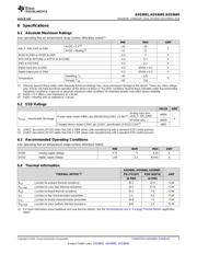
Oscillator
CONVST/CS
PGA
1 M:
OVP
1 M:
OVP
2
nd
-Order
LPF
ADC
Driver
V
BIAS
AIN_P
AIN_GND
4.096-V
Reference
REFGND
DGNDAGND
DVDD
AVDD
Digital Logic
and Interface
REFIO
REFCAP
SCLK
SDI
SDO
16-Bit
SAR ADC
ADS868x
Copyright © 2016, Texas Instruments Incorporated
Product
Folder
Sample &
Buy
Technical
Documents
Tools &
Software
Support &
Community
Reference
Design
An IMPORTANT NOTICE at the end of this data sheet addresses availability, warranty, changes, use in safety-critical applications,
intellectual property matters and other important disclaimers. PRODUCTION DATA.
ADS8681
,
ADS8685
,
ADS8689
SBAS633B –FEBRUARY 2016–REVISED DECEMBER 2016
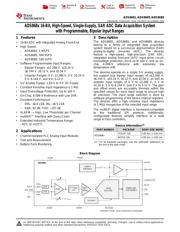
ADS868x 16-Bit, High-Speed, Single-Supply, SAR ADC Data Acquisition System
with Programmable, Bipolar Input Ranges
1
1 Features
1
• 16-Bit ADC with Integrated Analog Front-End
• High Speed:
– ADS8681: 1 MSPS
– ADS8685: 500 kSPS
– ADS8689: 100 kSPS
• Software Programmable Input Ranges:
– Bipolar Ranges: ±12.288 V, ±10.24 V,
±6.144 V, ±5.12 V, and ±2.56 V
– Unipolar Ranges: 0 V–12.288 V, 0 V–10.24 V,
0 V–6.144 V, and 0 V–5.12 V
• 5-V Analog Supply: 1.65-V to 5-V I/O Supply
• Constant Resistive Input Impedance ≥ 1 MΩ
• Input Overvoltage Protection: Up to ±20 V
• On-Chip, 4.096-V Reference with Low Drift
• Excellent Performance:
– DNL: ± 0.4 LSB; INL: ±0.5 LSB
– SNR: 92 dB; THD: –107 dB
• ALARM → High, Low Thresholds per Channel
• multiSPI™ Interface with Daisy-Chain
• Extended Industrial Temperature Range:
–40°C to +125°C
2 Applications
• Channel-Isolated PLC Analog Input Modules
• Test and Measurement
• Battery Pack Monitoring
3 Description
The ADS8681, ADS8685, and ADS8689 devices
belong to a family of integrated data acquisition
system based on a successive approximation (SAR)
analog-to-digital converter (ADC). The devices
feature a high-speed, high-precision SAR ADC,
integrated analog front-end (AFE) input driver circuit,
overvoltage protection circuit up to ±20 V, and an on-
chip 4.096-V reference with extremely low
temperature drift.
The devices operate on a single 5-V analog supply,
but support true bipolar input ranges of ±12.288 V,
±6.144 V, ±10.24 V, ±5.12 V, and ±2.56 V, as well as
unipolar input ranges of 0 V to 12.288 V, 0 V to
10.24 V, 0 V to 6.144 V, and 0 V to 5.12 V. The gain
and offset errors are accurately trimmed within the
specified values for each input range to ensure high
dc precision. The input range selection is done by
software programming of the device internal registers.
The devices offer a high resistive input impedance
(≥ 1 MΩ) irrespective of the selected input range.
The multiSPI digital interface is backward-compatible
to the traditional SPI protocol. Additionally,
configurable features simplify interface to a wide
range of host controllers.
Device Information
(1)
PART NUMBER PACKAGE BODY SIZE (NOM)
ADS868x
TSSOP (16) 5.00 mm × 4.40 mm
WQFN (16) 4.00 mm × 4.00 mm
(1) For all available packages, see the orderable addendum at
the end of the data sheet.
Block Diagram
页面指南