
下载
14-Bit, 1 MSPS, Unipolar/Bipolar
Programmable Input PulSAR
®
ADC
Data Sheet
AD7951
FEATURES
Multiple pins/software programmable input ranges:
5 V, 10 V, ±5 V, ±10 V
Pins or serial SPI® compatible input ranges/mode selection
Throughput
1 MSPS (warp mode)
800 kSPS (normal mode)
670 kSPS (impulse mode)
14-bit resolution with no missing codes
INL: ±0.3 LSB typ, ±1 LSB max (±61 ppm of FSR)
SNR: 85 dB @ 2 kHz
iCMOS® process technology
5 V internal reference: typical drift 3 ppm/°C; TEMP output
No pipeline delay (SAR architecture)
Parallel (14- or 8-bit bus) and serial 5 V/3.3 V interface
SPI-/QSPI™-/MICROWIRE™-/DSP-compatible
Power dissipation:
10 mW @ 100 kSPS
235 mW @ 1 MSPS
48-lead LQFP and LFCSP (7 mm × 7 mm) packages
APPLICATIONS
Process control
Medical instruments
High speed data acquisition
Digital signal processing
Instrumentation
Spectrum analysis
ATE
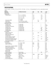
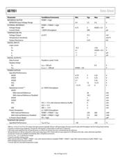
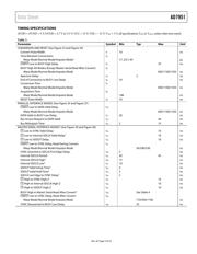
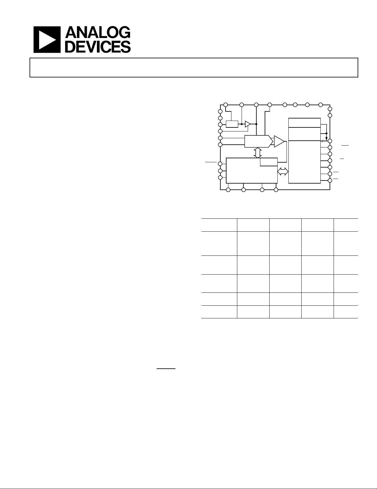
GENERAL DESCRIPTION
The AD7951 is a 14-bit, charge redistribution, successive
approximation register (SAR) architecture analog-to-digital
converter (ADC) fabricated on Analog Devices, Inc.’s iCMOS
high voltage process. The device is configured through hardware or
via a dedicated write only serial configuration port for input
range and operating mode. The AD7951 contains a high speed
14-bit sampling ADC, an internal conversion clock, an internal
reference (and buffer), error correction circuits, and both serial
and parallel system interface ports. A falling edge on
CNVST
samples the analog input on IN+ with respect to a ground
sense, IN−. The AD7951 features four different analog input
ranges and three different sampling modes: warp mode for the
fastest throughput, normal mode for the fastest asynchronous
throughput, and impulse mode where power is scaled with
throughput. Operation is specified from −40°C to +85°C.
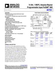
FUNCTIONAL BLOCK DIAGRAM
06396-001
14
CONTROL LOGIC AND
CALIBRATION CIRCUITRY
CLOCK
AD7951
DGND
DVDD
AVDD
AGND
REF REFGND
IN+
PD
RESET
CNVST
PDBUF
REFBUFIN
PDREF
REF
TEMP
D[13:0]
BUSY
RD
CS
OB/2C
OGND
OVDD
BYTES
WA
P
SER/PAR
REF
AMP
SERIAL DATA
PORT
PARALLEL
INTERFACE
SWITCHED
CAP DAC
VCC VEE
WARP
IMPULSE BIPOLAR
TEN
SERIAL
CONFIGURATION
PORT
IN–
Figure 1.
Table 1. 48-Lead 14-/16-/18-Bit PulSAR Selection
Type
100 kSPS to
250 kSPS
500 kSPS to
570 kSPS
570 kSPS to
1000 kSPS
>1000
kSPS
Pseudo
Differential
AD7651
AD7660
AD7661
AD7650
AD7652
AD7664
AD7666
AD7653
AD7667
True Bipolar
AD7610
AD7663
AD7665
AD7951
AD7612
AD7671
True
Differential
AD7675 AD7676 AD7677
AD7621
AD7622
AD7623
18-Bit, True
Differential
AD7678 AD7679 AD7674
AD7641
AD7643
Multichannel/
Simultaneous
AD7654
AD7655
Rev. B
Document Feedback
Information furnished by Analog Devices is believed to be accurate and reliable. However, no
responsibility is assumed by Analog Devices for its use, nor for any infringements of patents or other
rights of third parties that may result from its use. Specifications subject to change without notice. No
license is granted by implication or otherwise under any patent or patent rights of Analog Devices.
Trademarks and registered trademarks are the property of their respective owners.
One Technology Way, P.O. Box 9106, Norwood, MA 02062-9106, U.S.A.
Tel: 781.329.4700 ©2006–2015 Analog Devices, Inc. All rights reserved.
Technical Support www.analog.com
页面指南