
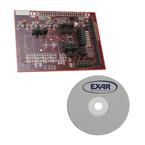
下载
1
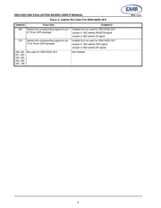
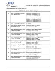
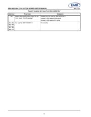
REV. 1.0.0 XRA1402/1404 EVALUATION BOARD USER’S MANUAL
INTRODUCTION
This user’s manual is for the XRA1402/1404 8-bit evaluation board. Table 1 shows the different devices and
packages that the evaluation board supports. This user’s manual will describe the hardware setup required to
operate the different packages.
1.0 QUICK START
To verify communication with the GPIO expander, the following steps are recommended:
1.1 Connect external +5V power supply to J8 pin 1
1.2 Connect J12 pin 13 and 14 to ground of external power supply
1.3 Connect to MCU SPI interface for:
SPI clock (SCK_SCL signal at J5 pin11)
SO (SO_SPI signal at J5 pin17)
SI (SI_SPI signal at J5 pin21)
CS# (CS#_SPI signal at J5 pin19)
1.4 From the MCU, write the following registers:
GCR = 0x00
If the LEDs turn on, the communication with the GPIO expander is successful.
To disable connection to LEDs, remove jumpers on J41 and J42. Connect to external inputs or outputs at
J1.
2.0 HARDWARE SETUP
2.1 Packages description
The evaluation board supports all 4 packages of the XRA1402 and XRA1404. The ordering part number,
package and location on the board is shown below in Table 1. Table 2 lists the evaluation board ordering part
numbers.
TABLE 1: PACKAGE LIST
ORDERING PART NUMBER PACKAGE LOCATION
XRA1402IL16-F 16-pin QFN U7
XRA1402IG16-F 16-pin TSSOP U6
XRA1404IL16-F 16-pin QFN U7
XRA1404IG16-F 16-pin TSSOP U6
TABLE 2: EVALUATION BOARD ORDERING PART NUMBERS
PART NUMBER
XRA1402IL16-0B-EB
XRA1402IG16-0B-EB
XRA1404IL16-0B-EB
XRA1404IG16-0B-EB