
下载
Product
Folder
Sample &
Buy
Technical
Documents
Tools &
Software
Support &
Community
TUSB1210
SLLSE09H –NOVEMBER 2009–REVISED JUNE 2015
TUSB1210 Stand-Alone USB Transceiver Chip Silicon
1 Device Overview
1.1 Features
1
Session Request Protocol (SRP)
• USB2.0 PHY Transceiver Chip, Designed to
Interface With a USB Controller Through a ULPI • V
BUS
Overvoltage Protection Circuitry Protects
Interface, Fully Compliant With: V
BUS
Pin in Range –2 V to 20 V
– Universal Serial Bus Specification Rev. 2.0 • Internal 5-V Short-Circuit Protection of DP, DM,
and ID Pins for Cable Shorting to V
BUS
Pin
– On-The-Go Supplement to the USB 2.0
Specification Rev. 1.3 • ULPI Interface:
– UTMI+ Low Pin Interface (ULPI) Specification – I/O Interface (1.8 V) Optimized for
Rev. 1.1 Nonterminated 50-Ω Line Impedance
– ULPI 12-pin SDR Interface – ULPI CLOCK Pin (60 MHz) Supports Both Input
and Output Clock Configurations
• DP/DM Line External Component Compensation
(Patent #US7965100 B1) – Fully Programmable ULPI-Compliant Register
Set
• Interfaces to Host, Peripheral and OTG Device
Cores; Optimized for Portable Devices or System • Full Industrial Grade Operating Temperature
ASICs With Built-in USB OTG Device Core Range From –40°C to 85°C
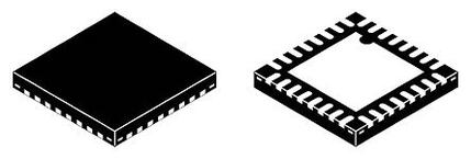
• Complete USB OTG Physical Front-End That • Available in a 32-Pin Quad Flat No Lead [QFN
Supports Host Negotiation Protocol (HNP) and (RHB)] Package
1.2 Applications
• Mobile Phones • Video Game Consoles
• Portable Computers • Desktop Computers
• Tablet Devices • Portable Music Players
1.3 Description
The TUSB1210 is a USB2.0 transceiver chip, designed to interface with a USB controller through a ULPI
interface. The device supports all USB2.0 data rates (high-speed 480 Mbps, full-speed 12 Mbps, and low-
speed 1.5 Mbps), and is compliant to both host and peripheral modes. The device additionally supports a
UART mode and legacy ULPI serial modes. TUSB1210 also supports the OTG (Ver1.3) optional
addendum to the USB 2.0 Specification, including HNP and SRP.
The DP/DM external component compensation in the transmitter compensates for variations in the series
impendence in order to match with the data line impedance and the receiver input impedance, to limit data
reflections and thereby improve eye diagrams.
Device Information
(1)
PART NUMBER PACKAGE BODY SIZE (NOM)
TUSB1210 VQFN (32) 5.00 mm x 5.00 mm
(1) For more information, see Section 8, Mechanical Packaging and Orderable Information.
1
An IMPORTANT NOTICE at the end of this data sheet addresses availability, warranty, changes, use in safety-critical applications,
intellectual property matters and other important disclaimers. PRODUCTION DATA.
页面指南