
下载

User's Guide
SLVU497A–August 2011–Revised February 2012
TPS62080, TPS62080A, 1.2-A, High-Efficiency, Step-Down
Converter in 2 x 2-mm SON Package
This user’s guide describes the TPS62080 evaluation module (EVM), how to perform a stand-alone
evaluation or interface with a host or system. The converter is designed to deliver up to 1200 mA of
continuous current to the output. The converter can be switched into snooze mode by pulling the mode pin
high. Snooze mode is typically used in system standby mode, results in better efficiency at light loads
(longer run time) at the expense of higher output ripple and reduced dynamic performance, which is often
a good tradeoff in this dormant system mode.
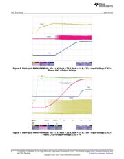
This EVM can support evaluation of either the TPS62080 or TPS62080A IC. The EVM is delivered with
the TPS62080 IC and the only difference between the two ICs is the discharge resistor that is internally
conected between the SW pin and the gound when the IC is disabled. The TPS62080 connects a 1k and
the TPS62080A connects a 50 Ω. To test with the 50 Ω discharge resistor, the IC can be replaced with
TPS62080A. When using TPS62080A, Figure 9 will have a faster discharge on V
OUT
.
1 Introduction
The TPS6208x focuses on high-efficiency, step-down conversion over a wide output current range. At
medium-to-heavy loads, the converter operates in PWM mode and automatically enters PFM or Power
Save mode operation at light-load currents to maintain high efficiency over the entire load current range.
To maintain high efficiency at low load or no load currents, a Snooze mode with an ultralow quiescent
current (5 µA) is implemented, which maintains the output voltage. This function increases the run-time of
battery- driven applications and keeps the standby current at its lowest level to meet green energy
standards targeting for a low standby current. To address the requirements of powering supply rails, the
internal compensation circuit allows a large selection of external output capacitor values ranging from 10
µF up to 100 µF. The TPS6208x operates at a nominal frequency of 3 MHz. With its DCS-Control™
architecture, excellent load transient performance, and output voltage regulation, accuracy is achieved.
The robust architecture and safety features allow perfect system integration. The device is available in 2 x
2-mm package with thermal PAD.
2 Considerations With Evaluating the TPS62080
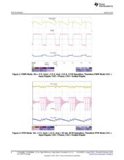
This integrated circuit (IC) has three modes of operation, the PWM/PFM mode is selected with the mode
pin low and is in PWM mode when the load current is greater than half the ripple current (in continuous
conduction mode). At light loads, when the inductor current is discontinuous, the IC automatically goes
into PFM mode and delivers fewer pulses, trying to keep a tight regulation with low ripple.
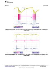
Pulling the mode pin high puts the IC in snooze mode, which uses far less power to operate at the
expense of higher ripple voltage and reduced transient performance.
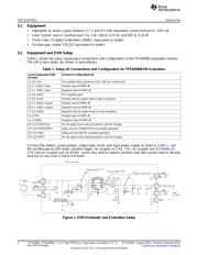
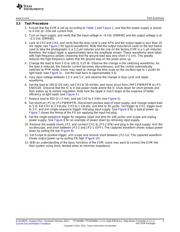
3 Test Summary
The TPS62080EVM-641 board requires an adjustable dc power supply with up to a 6-V output and ≥ 600
mA for powering the input to the EVM and a resistive output load between 825 Ω and 5 Ω. Choose the
proper power rating for the load resistor, P=V
2
/R. Use at least 2x the calculated power dissipation. The
test setup connections and jumper settings selections are configured for a stand-alone evaluation, but can
be changed to interface with external hardware such as a system load and microcontroller.
1
SLVU497A–August 2011–Revised February 2012 TPS62080, TPS62080A, 1.2-A, High-Efficiency, Step-Down Converter in 2 x 2-
mm SON Package
Submit Documentation Feedback
Copyright © 2011–2012, Texas Instruments Incorporated