
下载
Rev 1.4 4/16 Copyright © 2016 by Silicon Laboratories Si52143
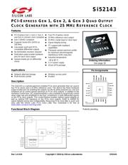
Si52143
PCI-EXPRESS GEN 1, GEN 2, & GEN 3 QUAD OUTPUT
C
LOCK GENERATOR WITH 25 MHZ REFERENCE CLOCK
Features
Applications
Description
The Si52143 is a spread-spectrum enabled PCIe clock generator that can source
four PCIe clocks and a 25 MHz reference clock. The device has three hardware
output enable pins for enabling the outputs (on the fly while powered on), and one
hardware pin to control spread spectrum on PCIe clock outputs. In addition to the
hardware control pins, I2C programmability is also available to dynamically control
skew, edge rate and amplitude on the true, compliment, or both differential signals
on the PCIe clock outputs. This control feature enables optimal signal integrity as
well as optimal EMI signature on the PCIe clock outputs. Refer to AN636 for
signal integrity tuning and configurability. Measuring PCIe clock jitter is quick and
easy with the Silicon Labs PCIe Clock Jitter Tool. Download it for free at
www.silabs.com/pcie-learningcenter.
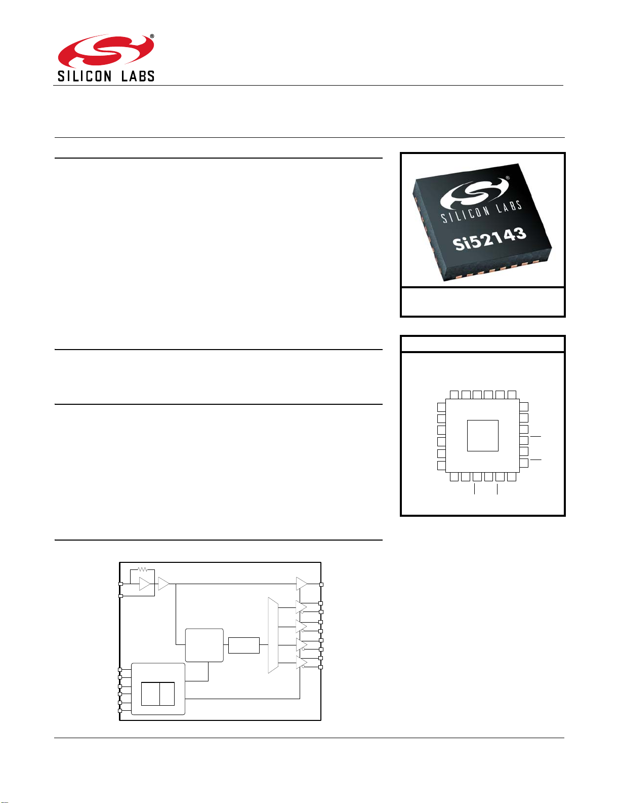
Functional Block Diagram
PCI-Express Gen 1, Gen 2, Gen 3,
and Gen 4 common clock compliant
Gen 3 SRNS Compliant
Supports Serial ATA (SATA) at
100 MHz
Low power, push-pull HCSL
compatible differential outputs
No termination resistors required
Dedicated output enable hardware
pins for each clock output
Spread enable pin on differential
clocks
Four PCI-Express clocks
25 MHz reference clock output
25 MHz crystal input or clock input
Signal integrity tuning
I
2
C support with readback
capabilities
Triangular spread spectrum profile
for maximum electromagnetic
interference (EMI) reduction
Industrial temperature
–40 to 85 °C
3.3 V power supply
24-pin QFN package
Network attached storage
Multi-function printer
Wireless access point
Routers
Control RAM
Control & Memory
XIN/CLKIN
XOUT
SCLK
SDATA
OE [3:2]
OE [1:0]
REF
OE_REF
SSON
DIFF1
DIFF3
DIFF0
PLL
(SSC)
Divider
DIFF2
Patents pending
Ordering Information:
See page 18
Pin Assignments
VDD_REF
REF
SSON
2
VSS_REF
VDD_DIFF
OE_REF
1
VSS_CORE
XIN/CLKIN
XOUT
1
2
3
4
5
6
24 23 22
21 20 19
7 8 9 10 11 12
18
17
16
15
14
13
OE[1:0]
1
DIFF0
DIFF0
DIFF1
DIFF1
VDD_DIFF
VDD_CORE
SDATA
SCLK
OE[3:2]
1
VDD_DIFF
DIFF3
DIFF3
DIFF2
DIFF2
Notes:
1. Internal 100 kohm pull-up.
2. Internal 100 kohm pull-down.
25
GND
页面指南