
下载

© Semiconductor Components Industries, LLC, 2010
April, 2010 − Rev. 7
1 Publication Order Number:
NCP3163/D
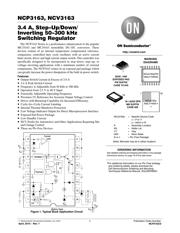
NCP3163, NCV3163
3.4 A, Step-Up/Down/
Inverting 50-300 kHz
Switching Regulator
The NCP3163 Series is a performance enhancement to the popular
MC33163 and MC34163 monolithic DC−DC converters. These
devices consist of an internal temperature compensated reference,
comparator, controlled duty cycle oscillator with an active current
limit circuit, driver and high current output switch. This controller was
specifically designed to be incorporated in step−down, step−up, or
voltage−inverting applications with a minimum number of external
components. The NCP3163 comes in an exposed pad package which
can greatly increase the power dissipation of the built in power switch.
Features
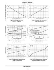
• Output Switch Current in Excess of 3.0 A
• 3.4 A Peak Switch Current
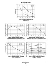
• Frequency is Adjustable from 50 kHz to 300 kHz
• Operation from 2.5 V to 40 V Input
• Externally Adjustable Operating Frequency
• Precision 2% Reference for Accurate Output Voltage Control
• Driver with Bootstrap Capability for Increased Efficiency
• Cycle−by−Cycle Current Limiting
• Internal Thermal Shutdown Protection
• Low Voltage Indicator Output for Direct Microprocessor Interface
• Exposed Pad Power Package
• Low Standby Current
• NCV Prefix for Automotive and Other Applications Requiring Site
and Change Control
• These are Pb−Free Devices
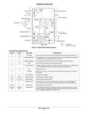
+
16
9
10
11
12
13
14
15
8
7
6
5
4
3
2
LVI
Oscillator
+
+
-
Current
Limit
Figure 1. Typical Buck Application Circuit
(Bottom View)
-
+
+
+
-
1
V
CC
V
CC
V
CC
V
in
C
in
Thermal
V
out
+
C
O
R
S
Q
See detailed ordering and shipping information in the package
dimensions section on page 18 of this data sheet.
ORDERING INFORMATION
MARKING
DIAGRAMS
NCx3163y = Specific Device Code
x = P or V
y = blank or B
A = Assembly Location
WL = Wafer Lot
YY = Year
WW = Work Week
G or G = Pb−Free Package
1
16
SOIC−16W
EXPOSED PAD
PW SUFFIX
CASE 751AG
http://onsemi.com
16
1
NCx3163yPW
AWLYYWWG
*For additional information on our Pb−Free strategy
and soldering details, please download the
ON Semiconductor Soldering and Mounting
Techniques Reference Manual, SOLDERRM/D.
18−LEAD DFN
MN SUFFIX
CASE 505
1
NCx3163y
AWLYYWW G
G
11
8
18
(Note: Microdot may be in either location)
页面指南