

下载

© Semiconductor Components Industries, LLC, 2016
January, 2016 − Rev. 0
1 Publication Order Number:
EVBUM2345/D
NCP1060FLBKGEVB
NCP1060 Flyback Converter
Evaluation Board
User'sManual
Universal AC Mains, Up to 7 Watt Isolated
Power Supply
Introduction
This evaluation board manual describes a simple, low
power (up to 7 W), universal AC mains Flyback converter.
The converter provides constant voltage output. The supply
can be used for powering utility electric meters, white goods
or similar industrial equipments where isolation from the
AC mains is required. The main benefits of provided
solution are high efficiency, cost effectiveness and low
no−load power consumption. The converter is utilizing
monolithic ON Semiconductor switcher NCP1060 with
integrated 34 W MOSFET in a PDIP7 package. The
evaluation board manual provides complete circuit diagram
and bill of materials. The current capability of provided
converter is user adjustable.
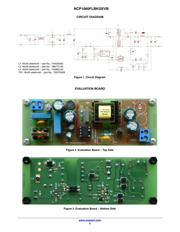
Circuit Description
The varistor R4 together with resistor R3 form simple
protection that enhances application robustness against line
over−voltage and voltage spikes. Resistor R3 also limits the
inrush current when the power supply is connected to mains.
The EMC filter is implemented to reduce conducted
electromagnetic emissions to the mains.
The Flyback converter itself is formed by the high voltage
switching regulator IC1, transformer TR1, freewheeling
diode D3 and coil L1 (L3). Capacitors C5, C6, C7 and C8 are
used as the output filtering and energy storage bank. Resistor
R1 and capacitor C2 for filter, C1, R2 and D2 are forming
voltage clamp for the switcher drain. Opto−coupler OK1
(NCP431) is used in feedback network. Resistors R8, R12
and R13 form resistive divider and sets output voltage.
Diode D7 and resistor R14 provide supply voltage for IC1
Vcc from auxiliary winding. The capacitor C10 is the energy
storage element that keeps IC1 powered during light load
conditions, when the switching frequency drops and energy
from auxiliary winding refills Vcc capacitors less often.
Pin LIM/OPP is connected through resistor R6 to
auxiliary winding and sets over−power protection. Resistor
R9 decreases maximal peak current. The frequency
compensation of the feedback loop system is ensured by
external capacitor C8 that is connected to the IC OTA output.
Key Features
• Universal AC Input Range (85 – 265 Vac)
• Input Filter for Conducted EMI Attenuation
• Very Low Standby and No−load Power Consumption
• Frequency Fold−back for Improved Efficiency at Light
Load
• Inherent Over−current, Over−voltage and
Over−temperature Protections
• Frequency Jittering for Better EMI Signature
• Adjustable Peak Current to Set the Required Level of
Over−current Protection
Table 1.
Description Output Specification
Output Voltage 12 Vdc
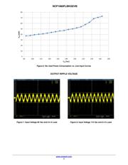
Output Ripple < 25 mV @ Full Load
Max Output Current 0.6 A
Min Output Current 0 A
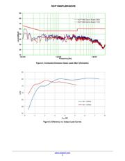
Efficiency See Efficiency Charts
Input Protection Fuse
Operating Temperature Range 0°C to +50°C
Cooling Method Passive Cooling
No−load Power Consumption < 75 mW @ 85 − 265 Vac
Table 2.
Device Application Input Voltage Output Power Topology I/O Isolation
NCP1060AP060G White Goods,
E−Meters
85 to 265 Vac 5 to 7 W Flyback Yes
www.onsemi.com
EVAL BOARD USER’S MANUAL