
下载
Semiconductor Components Industries, LLC, 2013
June, 2013 − Rev. 0
1 Publication Order Number:
EVBUM2191/D
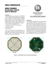
NB6L72MMNGEVB
NB6L72MMNG
Evaluation Board
User's Manual
Introduction
ON Semiconductor has developed the QFN16EVB
evaluation board for its high-performance devices packaged
in the 16-pin QFN. This evaluation board was designed to
provide a flexible and convenient platform to quickly
evaluate, characterize and verify the operation of various
ON Semiconductor products. Many QFN16EVBs are
dedicated with a device already installed, and can be ordered
from www.onsemi.com at the specific device web page.
This evaluation board manual contains:
Information on 16-lead QFN Evaluation Board
Assembly Instructions
Appropriate Lab Setup
Bill of Materials
This user’s manual provides detailed information on
board contents, layout and its use. It should be used in
conjunction with an appropriate ON Semiconductor device
datasheet located at www.onsemi.com. The datasheet
contains the technical device specifications.
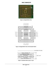
Board Layout
The QFN16 Evaluation Board provides a high bandwidth,
50 W controlled impedance environment and is
implemented in four layers. The first layer or primary trace
layer is 0.008 thick Rogers RO4003 material, and is
designed to have equal electrical length on all signal traces
from the device under test (DUT) pins to the SMA
connectors. The second layer is the 1.0 oz copper ground
plane and is primarily dedicated for the SMA connector
ground plane. FR4 dielectric material is placed between the
second and third layers and between third and fourth layers.
The third layer is also 1.0 oz copper plane. A portion of this
layer is designated for the device V
CC
and DUTGND power
planes. The fourth layer is the secondary trace layer.
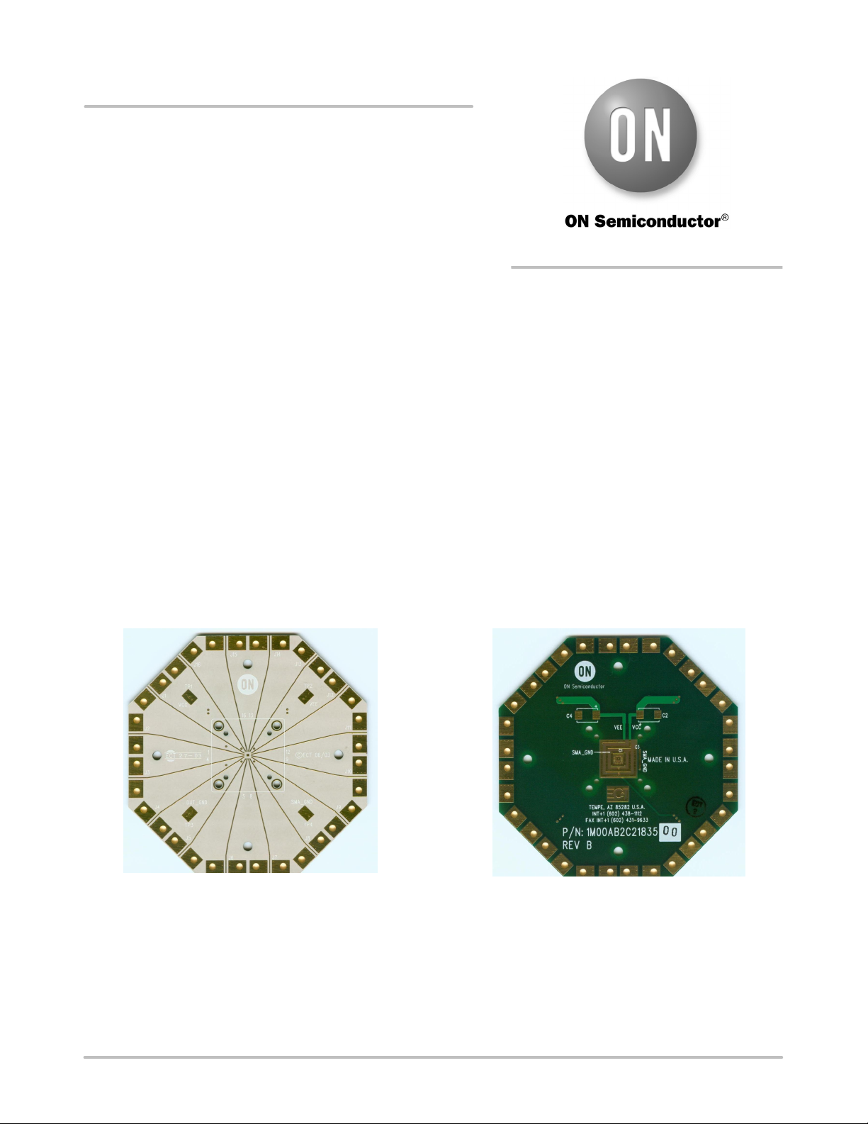
Figure 1. Top and Bottom View of the 16 QFN Evaluation Board
Top View Bottom View
http://onsemi.com
EVAL BOARD USER’S MANUAL