
下载

© Semiconductor Components Industries, LLC, 2012
April, 2012− Rev. 3
1 Publication Order Number:
EVBUM2082/D
NB6L295MNGEVB,
NB6L295MMNGEVB
NB6L295MNG/
NB6L295MMNG Evaluation
Board User's Manual
Introduction and Board Description
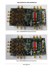
The NB6L295M Evaluation Board was designed to
provide a flexible and convenient platform to quickly
evaluate, characterize and verify the operation and
performance of either the NB6L295MMNG (CML) or the
NB6L295MNG (LVPECL) Dual Channel Programmable
Delay.
This evaluation board manual contains:
• Information on the NB6L295M Evaluation Board
• Appropriate Lab Setup
• Detailed Board Features
• Bill of Materials
This manual should be used in conjunction with the device
datasheet NB6L295M/D or NB6L295/D which contains full
technical details on the device specifications and operation.
The NB6L295M Evaluation Board was also designed to
accommodate a custom QFN−24 socket. Therefore, some
external components were installed on the bottom side of the
board.
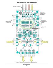
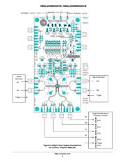
Board Features
• On board programmable SDI circuitry minimizing
cabling, or, external SDI accessed through SMA
connectors.
• Convenient and compact board layout
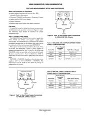
• 2.5 V or 3.3 V single or split−power supply operation
(banana jack connectors for VCC, SMAGND and
DUTGND; Separate PLDVCC power supply for on
board PLD
• CML or LVPECL differential output signals are
accessed via SMA connectors with provision for load
termination resistors
• SMA connectors are provided for 1) all high−speed
differential input & (CML or LVPECL) output signals
and 2) for external SDI & control signals access
Board Layout
The evaluation board is constructed in four layers. The top
layer is the primary trace layer and is made with polyimide
material. This layer provides a high−bandwidth 50 W
controlled trace impedance environment for the equal length
inputs and outputs. The second layer is a copper ground
plane.
Layer Stack
L1 Signal − “High and Low Speed”
L2 SMA Ground
L3 VCC (Device positive power supply) and DUTGND
(Device negative power supply)
L4 Signal − “Low Speed”
What measurements can you expect to make?
With this evaluation board, the following measurements
could be performed in single ended or differential modes of
operation.
• Propagation and Programmed Delay
• Output Rise and Fall Time
• Frequency Performance
• Jitter
• VCMR − Common Mode Range
http://onsemi.com
EVAL BOARD USER’S MANUAL