
下载
© Semiconductor Components Industries, LLC, 2015
April, 2015− Rev. 13
1 Publication Order Number:
NB100LVEP222/D
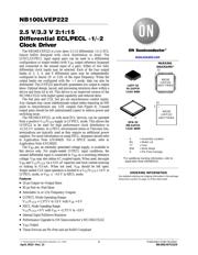
NB100LVEP222
2.5 V/3.3 V 2:1:15
Differential ECL/PECL ÷1/÷2
Clock Driver
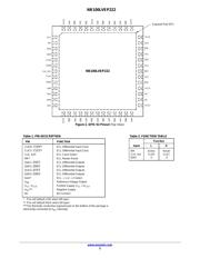
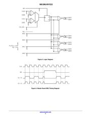
The NB100LVEP222 is a low skew 2:1:15 differential ÷1/÷2 ECL
fanout buffer designed with clock distribution in mind. The
LVECL/LVPECL input signal pairs can be used in a differential
configuration or single−ended (with V
BB
output reference bypassed
and connected to the unused input of a pair). Either of two fully
differential clock inputs may be selected. Each of the four output
banks of 2, 3, 4, and 6 differential pairs may be independently
configured to fanout 1X or 1/2X of the input frequency. When the
output banks are configured with the B1 mode, data can also be
distributed. The LVEP222 specifically guarantees low output to output
skew. Optimal design, layout, and processing minimize skew within a
device and from lot to lot. This device is an improved version of the
MC100LVE222 with higher speed capability and reduced skew.
The fsel pins and CLK_Sel pin are asynchronous control inputs.
Any changes may cause indeterminate output states requiring an MR
pulse to resynchronize any 1/2X outputs (See Figure 4). Unused
output pairs should be left unterminated (open) to reduce power and
switching noise.
The NB100LVEP222, as with most ECL devices, can be operated
from a positive V
CC
/V
CC0
supply in LVPECL mode. This allows the
LVEP222 to be used for high performance clock distribution in
+2.5/3.3 V systems. In a PECL environment series or Thevenin line,
terminations are typically used as they require no additional power
supplies. For more information on using PECL, designers should refer
to Application Note AN1406/D. For a SPICE model, refer to
Application Note AN1560/D.
The V
BB
pin, an internally generated voltage supply, is available to
this device only. For single−ended LVPECL input conditions, the
unused differential input is connected to V
BB
as a switching reference
voltage. V
BB
may also rebias AC coupled inputs. When used, decouple
V
BB
and V
CC
/V
CC0
via a 0.01 mF capacitor and limit current sourcing
or sinking to 0.5 mA. When not used, V
BB
should be left open.
Single−ended CLK input operation is limited to a V
CC
/V
CC0
≥ 3.0 V in
LVPECL mode, or V
EE
v −3.0 V in NECL mode.
Features
• 20 ps Output−to−Output Skew
• 85 ps Part−to−Part Skew
• Selectable 1x or 1/2x Frequency Outputs
• LVPECL Mode Operating Range:
V
CC
/V
CC0
= 2.375 V to 3.8 V with V
EE
= 0 V
• NECL Mode Operating Range:
V
CC
/V
CC0
= 0 V with V
EE
= −2.375 V to −3.8 V
• Internal Input Pulldown Resistors
• Performance Upgrade to ON Semiconductor’s MC100LVE222
• V
BB
Output
• These Devices are Pb−Free and are RoHS Compliant
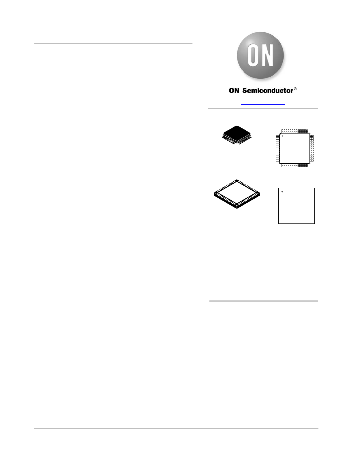
www.onsemi.com
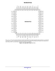
LQFP−52
FA SUFFIX
CASE 848H
MARKING
DIAGRAMS*
*For additional marking information, refer to
Application Note AND8002/D.
See detailed ordering and shipping information in the packag
e
dimensions section on page 11 of this data sheet.
ORDERING INFORMATION
A = Assembly Location
WL = Wafer Lot
YY = Year
WW = Work Week
G = Pb−Free Package
NB100
LVEP222
AWLYYWWG
1
QFN−52
MN SUFFIX
CASE 485M
152
NB100
LVEP222
AWLYYWWG
1
52
52
页面指南