
下载
AN3778
1
RF Application Information
Freescale Semiconductor
PCB Layout Guidelines for PQFN/QFN Style
Packages Requiring Thermal Vias for Heat
Dissipation
By: Quan Li, Lu Li, R ichard Rowan, and Mahesh Shah
PURPOSE
This document provides guidelines for printed circuit board
(PCB) designs for Power Quad Flat No--Lead (PQFN/QFN)
packages soldered on thermal via. RF power devices typically
generate heat that must be conducted away from the device.
The heat source is on the die, and the die is located on the die
flag or exposed heat spreader. To dissipate this heat through
the PCB, the exposed heat spreader is attached to a center
pad with via holes. The center pad is surrounded by peripheral
pads that correspond to the peripheral leads of the device. The
specific guidelines explained here are for RF power devices
with PQFN and QFN packages (e.g., Case Outline Nos. 1894,
1543, 1898, etc.). These devices require an extensive thermal
via structure in the PCB center pad area for thermal
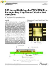
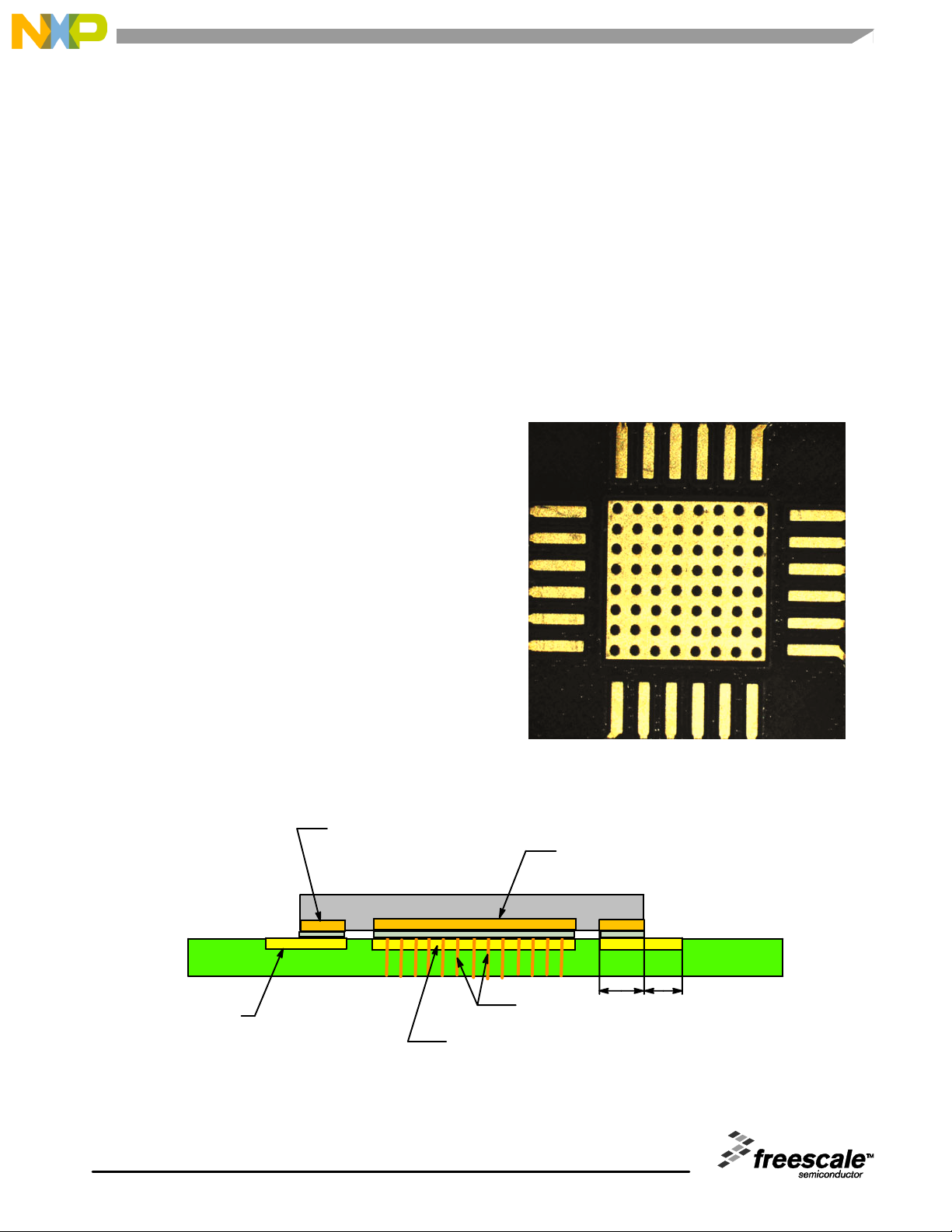
management. Figure 1 shows a typical PCB layout for this
type of package showing via holes in the center pad as well as
six peripheral pads, each on all four sides of the center pad.
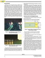
Figure 2 shows a typical cross--section of an RF Power device
in a PQFN package surface mounted on the PCB. Freescale
Application Note AN2467 for Power Quad Flat No--Lead
(PQFN) packages provides necessary guidelines for
designing the PCB layout for a typical PQFN package. The
application note also covers reliability test results for solder
joints when the guidelines are followed. This application note
provides supplemental information to AN2467, and includes
special requirements for devices that require thermal vias in
the center pad.
Figure 1. Typical PCB Layout for 8x8
PQFN--24 Package
PQFN
EXPOSED HEAT SPREADER
PERIPHERAL LEADS
PCB
THERMAL VIA
CENTER PAD WITH THERMAL VIA
(SAME SIZE AS HEAT SPREADER)
ad
PERIPHERAL
PADS
Figure 2. Typical Cross--section of PQFN Package for RF Power Device
Surface Mounted on a PCB
AN3778
Rev. 0, 2/2010
Freescale Semiconductor
Application Note
! Freescale Semiconductor , Inc., 2010.
A
ll rights reserved.