
下载
1
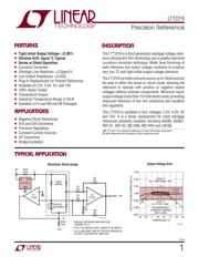
LT1019
1019fd
Precision Reference
The LT
®
1019 is a third generation bandgap voltage refer-
ence utilizing thin film technology and a greatly improved
curvature correction technique. Wafer level trimming of
both reference and output voltage combines to produce
very low TC and tight initial output voltage tolerance.
The LT1019 can both sink and source up to 10mA and can
be used in either the series or shunt mode, allowing the
reference to operate with positive or negative output
voltages without external components. Minimum input/
output voltage is less than 1V in the series mode, providing
improved tolerance of low line conditions and excellent
line regulation.
The LT1019 is available in four voltages: 2.5V, 4.5V, 5V
and 10V. It is a direct replacement for most bandgap
references presently available including AD580, AD581,
REF-01, REF-02, MC1400, MC1404 and LM168.
■
Tight Initial Output Voltage: <0.05%
■
Ultralow Drift: 3ppm/°C Typical
■
Series or Shunt Operation
■
Curvature Corrected
■
Ultrahigh Line Rejection: ≈ 0.5ppm/V
■
Low Output Impedance: ≈ 0.02Ω
■
Plug-In Replacement for Present References
■
Available at 2.5V, 4.5V, 5V, and 10V
■
100% Noise Tested
■
Temperature Output
■
Industrial Temperature Range in SO-8
■
Available in 8-Lead N8 and S8 Packages
■
Negative Shunt References
■
A/D and D/A Converters
■
Precision Regulators
■
Constant Current Sources
■
V/F Converters
■
Bridge Excitation
Ultralinear Strain Gauge
Output Voltage Drift
FEATURES
DESCRIPTIO
U
APPLICATIO S
U
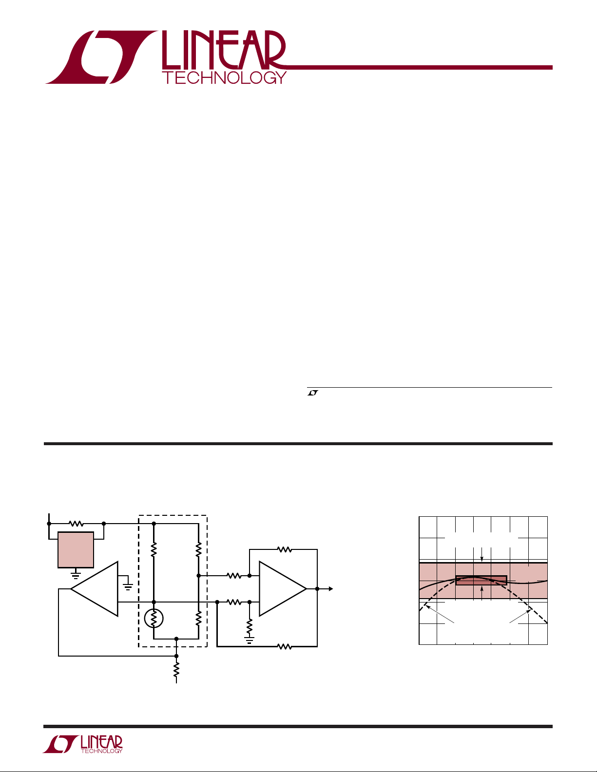
TYPICAL APPLICATION
U
–
+
A1
†
LT1637
–
+
A2
LT1001
R3
2M
R2
20k
R4
20k
GAIN = 100
R5
2M
R6**
2M
IN
LT1019-5
GND
OUT
15V
5V
357Ω*
0.5W
ACTIVE
ELEMENT
350Ω
BRIDGE
–15V
–5V
357Ω*
0.5W
REDUCES REFERENCE AND AMPLIFIER
LOADING TO ≈0.
IF R6 = R3, BRIDGE IS NOT LOADED BY R2 AND R4.
A1 V
OS
AND DRIFT ARE NOT CRITICAL BECAUSE A2
ACTS AS A DIFFERENTIAL AMPLIFIER.
*
**
†
LT1019 • TA01
TEMPERATURE (˚C)
–50
OUTPUT VOLTAGE (NORMALIZED) (V)
1.001
1.002
1.003
25 75
1019 TA02
1.000
0.999
–25 0
50 100 125
0.998
0.997
5ppm/°C
0°C TO 70°C “BOX”
LT1019
CURVE
UNCOMPENSATED
“STANDARD” BANDGAP
DRIFT CURVE
10ppm/°C
FULL TEMP RANGE “BOX”
, LTC and LT are registered trademarks of Linear Technology Corporation.
All other trademarks are the property of their respective owners.