
下载
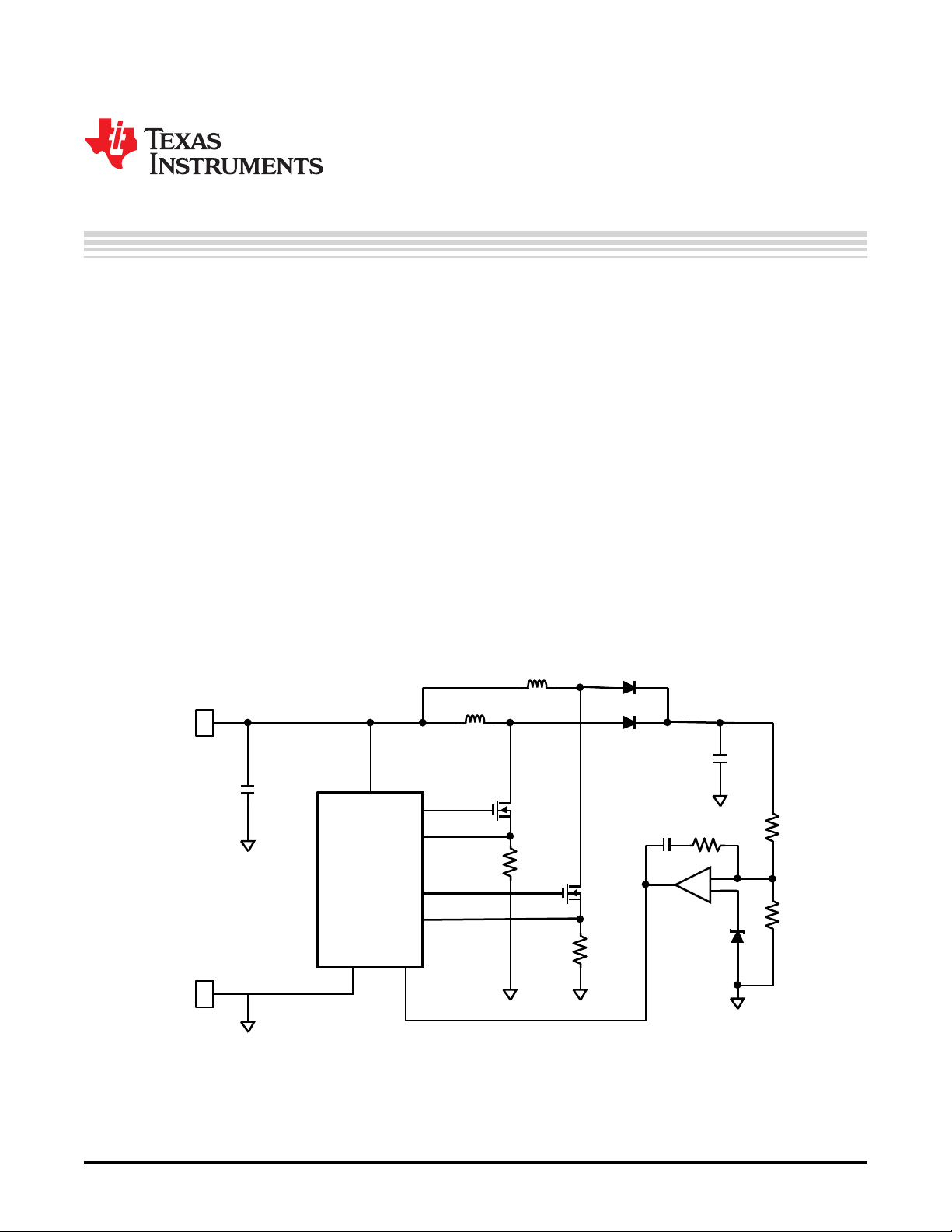
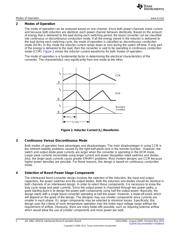
LM5032
+
-
D1
D2
Q2
Q1
Rs1
Rs2
U2
U1
L1
L2
REF
Cout
Cin
Vin
Gnd
User's Guide
SNVA395A–August 2009–Revised May 2013
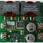
AN-1962 LM5032 Interleaved Boost Evaluation Board
The LM5032 dual current mode PWM controller contains all the features needed to control an interleaved
boost converter. The two outputs operate 180 degrees out of phase and have separate current limit inputs
for each channel. In addition to a high input voltage range, the controller contains all the auxiliary features
needed to control a complete converter.
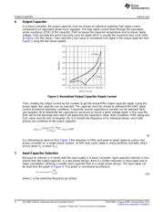
1 Introduction
A basic boost converter converts a DC voltage to a higher DC voltage. Interleaving adds additional
benefits such as reduced ripple currents in both the input and output circuits. Higher efficiency is realized
by splitting the output current into two paths, substantially reducing I
2
R losses and inductor AC losses.
Figure 1 shows the basic interleaved boost topology.
When Q1 turns on, current ramps up in L1 with a slope depending on the input voltage, storing energy in
L1. D1 is off during this time since the output voltage is greater than the input voltage. Once Q1 turns off,
D1 conducts delivering part of its stored energy to the load and the output capacitor. Current in L1 ramps
down with a slope dependent on the difference between the input and output voltage. One half of a
switching period later, Q2 also turns on completing the same cycle of events. Since both power channels
are combined at the output capacitor, the effective ripple frequency is twice that of a conventional single
channel boost regulator.
Figure 1. Interleaved Boost Basic Diagram
All trademarks are the property of their respective owners.
1
SNVA395A–August 2009–Revised May 2013 AN-1962 LM5032 Interleaved Boost Evaluation Board
Submit Documentation Feedback
Copyright © 2009–2013, Texas Instruments Incorporated