
下载
User's Guide
SNVA365E–September 2008–Revised April 2013
AN-1891 LM22679 Evaluation Board
1 Introduction
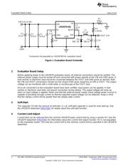
The LM22679 evaluation board is designed to demonstrate the capabilities of the LM22679 switching
regulator. The LM22679 evaluation board schematic shown in Figure 1 is configured to provide an output
voltage of 3.3V up to 5A load current with an input voltage range of 4.5V to 42V. Due to the low R
DS(ON)
of
the integrated N-channel MOSFET and maximum duty-cycle limitations, the minimum input voltage of
4.5V will only provide a 3.3V output voltage for load currents up to 500 mA. At 5.5V input voltage 3A of
output current is possible while maintaining 3.3V of output voltage. For load currents higher than 3A, an
input voltage of 6.5V or higher is required. The typical operating frequency is 500 kHz. The evaluation
board is designed to operate at ambient temperatures up to 30°C.
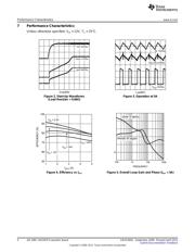
The performance of the evaluation board is as follows:
• Input Range: 4.5V to 42V
• Output Voltage: 3.3V
• Output Current Range: 0A to 5A
• Frequency of Operation: 500 kHz
• Board Size: 2.25 × 2 inches (57 mm × 50.5 mm)
• Package: TO-263 THIN
At low input voltages between 4.5V and 6V, a minimum load of approximately 5 mA may be required to
reach a regulated 3.3V output voltage. For more details, see LM22679/LM22679Q 42V, 5A SIMPLE
SWITCHER Step-Down Voltage Regulator with Features (SNVS581).
To aid in the design and evaluation of DC/DC buck converter solutions based on the LM22679 switching
regulator, the evaluation board can be re-configured for different output voltages.
The evaluation board is designed to highlight applications with a small solution size. This implies that there
will be a tradeoff with the area of heat dissipation available. If this evaluation board is operated
continuously at a full 5A load, it will get hot. For higher output voltages than the pre-adjusted 3.3V, the
total output power as well as the total power conversion losses will increase. It is recommended to use a
fan or other source of air flow when evaluating the board at full 5A load or at output voltages greater than
3.3V. Typical evaluation board performance and characteristics curves are shown in Section 7. The PCB
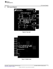
layout is shown in Section 8.
Test points are provided to enable easy connection and monitoring of critical signals. When performing
over load or short circuit tests, refer to the current limit section of the LM22679 datasheet (SNVS581) to
determine if the circuit is in safe operating mode.
For more information about device function and electrical characteristics, refer to the LM22679 datasheet
(SNVS581).
WEBENCH is a registered trademark of Texas Instruments.
All other trademarks are the property of their respective owners.
1
SNVA365E–September 2008–Revised April 2013 AN-1891 LM22679 Evaluation Board
Submit Documentation Feedback
Copyright © 2008–2013, Texas Instruments Incorporated