
下载
3-1
TM
AN9707
1-888-INTERSIL or 321-724-7143 | Intersil and Design is a trademark of Intersil Corporation. | Copyright © Intersil Corporation 2000
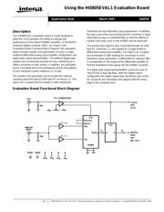
Using the HI5805EVAL1 Evaluation Board
Description
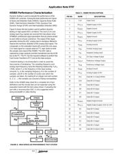
The HI5805EVAL1 evaluation board is made available to
allow the circuit designer the ability to evaluate the
performance of the Intersil HI5805 monolithic 12-bit 5MSPS
analog-to-digital converter (ADC). As shown in the
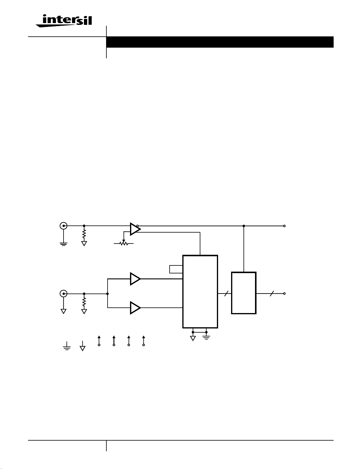
Evaluation Board Functional Block Diagram, this evaluation
board includes sample clock generation circuitry, a single-
ended to differential analog input amplifier configuration and
digital data output latches/buffers. The buffered digital data
outputs are conveniently provided for easy interfacing to a
ribbon connector or logic probes. In addition, the evaluation
board is provided with some prototyping area for the addition
of user designed custom interfaces or circuits.
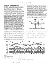
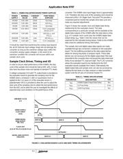
The sample clock generator circuit accepts the external
sampling signal through an SMA type RFconnector, J2.This
input is AC-coupled and terminated in 50W allowing for
connection to most laboratory signal generators. In addition,
the duty cycle of the clock driving the A/D converter is made
adjustable by way of a potentiometer so that the effects of
sample clock duty cycle on the HI5805 may be observed.
The analog input signal is also connected through an SMA
type RF connector, J1, and applied to a single-ended to
differential analog input amplifier. This input is AC-coupled
and terminated in 50W allowing for connection to most
laboratory signal generators. A differential RC lowpass filter
is incorporated on the output of the differential amplifier to
limit the broadband noise going into the HI5805 converter.
The digital data output latches/buffers consist of a pair of
74ALS574A D-type flip-flops. With this digital output
configuration the digital output data transitions seen at the
I/O connector are essentially time aligned with the rising
edge of the sampling clock.
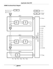
Evaluation Board Functional Block Diagram
CLK
+5V
D
-5V
D
V
REFOUT
V
REFIN
V
IN-
G = +1
TTL COMPARATOR
12
CLOCK
DIGITAL
DGND
AGND
D
0
-D
11
HI5805
ANALOG
50Ω
+5V
D
-5V
D
+5V
A
-5V
A
50Ω
CLK
D
Q
OUT
DATA
V
IN+
CLK
INPUT
OUT
12
(CLK)
(D0 - D11)
G = -1
Application Note March 1997