
下载
DS50EV401-EVK User Guide
February 2008
© National Semiconductor Corporation
DS50EV401-EVK User Guide
2.5 Gbps / 5.0 Gbps / 8.0 Gbps Quad PCI Express Cable and PC Board Equalizer
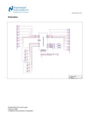
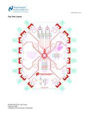
Overview
The DS50EV401-EVK evaluation board provides a typical PCIe application for the evaluation of the DS50EV401
2.5 Gbps, 5 Gbps, 8 Gbps x4 Lane Serial PCI Express Equalizer.
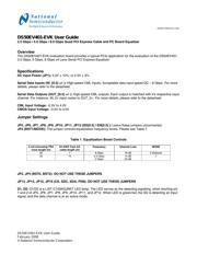
Specifications
DC Input Power (JP1): 3.3V ± 10%, or 2.5V ± 5%
Serial Data Inputs (IN_[0:3] +/- ): High-speed CML inputs. Acceptable data input speed DC – 8 Gbps. For more
details, please refer to the datasheet.
Serial Data Outputs (OUT_[0:3] +/- ): High-speed CML outputs. Each output is matched with it’s respective input
channel. For instance, IN_0+ input routes to OUT_0+. For more details, please refer to the datasheet.
CML Input Voltage: -0.5V to 4.0V
CMOS Input Voltage: -0.5V to 4.0V
Jumper Settings
JP5, JP6, JP7, JP8, JP9, JP10, JP11, JP12 (SD[0:3] / EN[0:3] ): Leave these jumpers unconnected.
JP3 (BST1/MODE): The jumper controls equalization frequency levels. Please see Table 1.
Table 1. Equalization Boost Controls
6 mil microstrip FR4
trace length (in)
24 AWG Twin-AX
cable length (m)
Frequency Channel Loss MODE
30 7 8 Gbps 16 dB 0 (Default)
40 10 2.5 Gbps
5 Gbps
14 dB
20 dB
1
JP2, JP4 (BST0, BST2): DO NOT USE THESE JUMPERS
JP13, JP14, JP15, JP16 (CS, SDC, SDA, FEB): DO NOT USE THESE JUMPERS
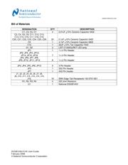
D1, D2: D1/D2 is a LIST-C155KGJRKT LED lamp. The LED serves as the detecting signaling, when shorting pin
1 and 2 of JP5, JP6, JP7, JP8, JP9, JP10, JP11, and JP12. When LED is green/red, the SD is detecting an input
signal, and the data channel is at an active mode.