
下载

Maxim > Design Support > Technical Documents > Application Notes > Microcontrollers > APP 93
Keywords: secure microcontroller, nonvolatile SRAM, NVSRAM, high-speed microcontroller,
microcontrollers, DS5000, DS5000T, DS5000FP, DS5001FP, DS5002FP, DS2250, DS2250T, DS2251T,
DS2252T, DS5230, DS5250, DS87C530
APPLICATION NOTE 93
Design Guidelines for Microcontrollers
Incorporating NV RAM
By: Kevin Self
May 01, 2001
Abstract: This application note will help the user of the Dallas Semiconductor secure microcontroller and
high-speed microcontroller improve reliability when implementing nonvolatile SRAM. This note is
applicable to the Secure and High-Speed Secure Microcontroller families as well as the DS87C530 high-
speed microcontroller. Out-of-tolerance voltage spikes, protecting I/O pins and negative power supply
transients are discussed in this application note.
Overview
Microcontrollers which incorporate battery-backed, nonvolatile SRAM (NV RAM) have found wide
acceptance in the embedded marketplace. Unlike Flash memory or EEPROM technology, nonvolatile
SRAM has no write limitations, which makes it ideal for real-time data logging applications. In products
such as the Dallas Semiconductor Secure Microcontroller family, NV RAM can be used to provide
insystem reprogrammable program memory.
This application note discusses design guidelines for microcontroller products which incorporate NV
RAM. A number of design suggestions are presented to improve the reliability of microcontrollers which
incorporate NV RAM. It should be stressed that battery-backed memory is as reliable as nonvolatile
memory as long as standard CMOS design guidelines are used. This application note is applicable to the
Secure and High-Speed Secure Microcontroller family of products as well as the DS87C530 High-Speed
Microcontroller.
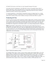
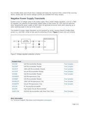
Out-of-Tolerance Voltage Spikes
The real world is a harsh place; electrostatic discharge (ESD), electrical noise, etc. can enter into a
system. Many of these phenomena can induce negative voltages on one or more device pins. CMOS
design guidelines require that no pin be taken above V
CC
or below V
SS
. Violation of this guideline can
result in a hard failure (damage to the silicon inside the device) or a soft failure (unintentional
modification of memory contents).
Negative voltage spikes are a particular problem for CMOS devices. When a negative voltage spike is
experienced, one or more parasitic diodes inside the device can become forward-biased. This will cause
the device to consume a large amount of current, and can cause the device to latch-up. In general, the
only way to reverse CMOS latch-up is to remove power from the device. If the supply to the device is
Page 1 of 4