

下载

User's Guide
SLAU203 – February 2007
ADS8472EVM
This user guide describes the characteristics, operation, and use of the ADS8472 16-bit, 1MHz parallel
interface analog-to-digital converter evaluation board. A complete circuit description as well as schematic
diagram and bill of materials is included.
Contents
1 EVM Overview ............................................................................................................... 2
2 Introduction ................................................................................................................... 2
3 Analog Interface .............................................................................................................. 2
4 Digital Interface .............................................................................................................. 5
5 Power Supplies .............................................................................................................. 7
6 Using the ADS8472EVM .................................................................................................... 8
7 ADS8472EVM BoM ........................................................................................................ 10
8 ADS8472EVM Layout ..................................................................................................... 12
9 ADS8472EVM Schematic ................................................................................................. 15
List of Figures
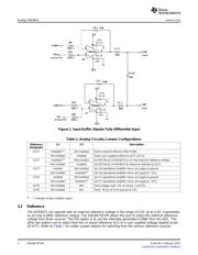
1 Input Buffer, Bipolar Fully Differential Input .............................................................................. 4
2 Top – Layer 1 ............................................................................................................... 12
3 Ground Plane – Layer 2 ................................................................................................... 13
4 Power Plane – Layer 3 .................................................................................................... 13
5 Bottom – Layer 4 ........................................................................................................... 14
6 Top Overlay ................................................................................................................ 14
7 Bottom OverLay ............................................................................................................ 15
List of Tables
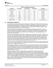
1 Analog Input Connector ..................................................................................................... 3
2 Analog Circuitry Jumper Configurations .................................................................................. 4
3 Pinout for Parallel Control Connector P3 ................................................................................. 5
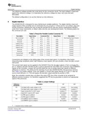
4 Jumper Settings .............................................................................................................. 5
5 Data Bus Connector P2 ..................................................................................................... 6
6 TSW1100 Connector ........................................................................................................ 6
7 Pin out for Converter Control Connector, J6 ............................................................................. 7
8 Power Supply Test Points .................................................................................................. 7
9 Power Connector, J5, Pin Out ............................................................................................. 7
10 Bill of Materials ............................................................................................................. 10
SLAU203 – February 2007 ADS8472EVM 1
Submit Documentation Feedback