


下载

AN-941
APPLICATION NOTE
One Technology Way • P. O. Box 9106 • Norwood, MA 02062-9106, U.S.A. • Te l: 781.329.4700 • Fax: 781.461.3113 • www.analog.com
ADN2817/ADN2818 BER Monitor and Sample Phase Adjust User Guide
by Eric Evans
Rev. PrA | Page 1 of 29
INTRODUCTION
The ADN2817/ADN2818 provide a bit error rate (BER) measure-
ment feature for estimating the actual BER of the IC. The feature
also allows data eye jitter profiling and Q-factor estimation.
Other capabilities offered include:
The ability to scan a region of the input data eye, which
is offset from the actual sampling instant, to build up a
pseudo bit error ratio profile.
The ability to apply algorithms to process this data to
obtain an accurate estimate of the BER at the actual
sampling instant. User processing of the data results
in greater accuracy and flexibility. A standby mode
conserves power.
Decomposition into random jitter (RJ) and deterministic
jitter (DJ). The dual-Dirac model is used for DJ.
Voltage output mode provides indication of BER and eye
opening.
Sample phase adjust ability. This mode is not concurrent
with BER monitoring.
Understanding the BER of the circuit is useful for the following
applications:
BER monitoring indicates the onset of laser fading, and
slow system degradation.
Margin measurement, which is the difference between
received SNR and the SNR required to guarantee a certain
BER, such as 1e−10.
Driving adaptive equalizers.
Sample phase adjust
Optimum slice threshold adjust (ADN2817 only).
Determination of dominant noise sources, that is,
independent of power, proportional to √power, and
proportional to power.
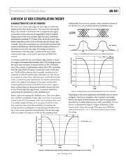
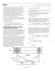
Circuitry within the ADN2817/ADN2818 allows measurement
of the pseudo bit error ratio at phases that are offset from the
actual sampling instant by more than approximately 0.05 UI.
The implementation relies on the fact that by knowing the BER
at sampling phases offset from the ideal sampling phase, it is
possible to extrapolate to obtain an estimate of the BER at the
actual sampling instant. This extrapolation relies on the assump-
tion that the input jitter is composed of deterministic and
random (Gaussian) components.
See the References section for resources that provide further
information on BER estimation. The implementation requires
off-chip control and data processing to estimate the actual BER.
Additionally, there is a lower accuracy voltage output mode,
which does not requires user processing or I
2
C intervention.