

下载
Evaluation Board User Guide
UG-337
One Technology Way • P. O. Box 9106 • Norwood, MA 02062-9106, U.S.A. • Tel: 781.329.4700 • Fax: 781.461.3113 • www.analog.com
Universal Evaluation Board for Dual, High Speed Op Amps
Offered in 10-Lead MSOP Packages
PLEASE SEE THE LAST PAGE FOR AN IMPORTANT
WARNING AND LEGAL TERMS AND CONDITIONS.
Rev. 0 | Page 1 of 8
FEATURES
Enables quick breadboarding/prototyping
User defined circuit configuration
Edge mounted SMA connector provisions
Easy connection to test equipment and other circuits
GENERAL DESCRIPTION
The Analog Devices, Inc., dual, 10-lead MSOP universal evalu-
ation board is designed to help users evaluate dual, high speed
op amps offered in 10-lead mini small outline packages (MSOP).
The dual MSOP board is a bare board (that is, no components
are soldered to the board) that enables users to quickly prototype
a variety of dual op amp circuits, thereby minimizing risk and
reducing time to market.
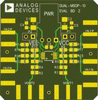
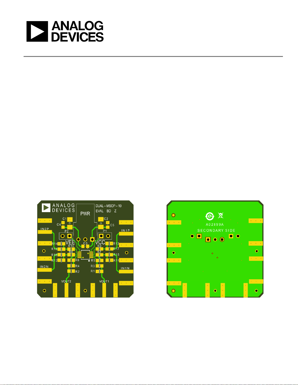
Figure 1 shows the component side of the bare evaluation board,
and Figure 2 shows the solder side of the evaluation board.
The evaluation board is a 6-layer printed circuit board (PCB)
that accepts SMA edge mounted connectors on the inputs and
outputs for efficient connection to test equipment or other circuitry.
The ground plane and component placement are designed to
minimize parasitic inductances and capacitances. The evaluation
board components are primarily 0603 case size, with the exception
of the electrolytic bypass capacitors (C1 and C2), which are
1206 case size.
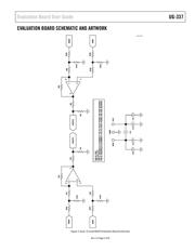
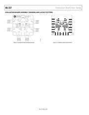
Figure 3 shows the evaluation board schematic. Figure 4 and
Figure 5 show the assembly drawing and the layout pattern of
the component side, respectively. The bill of materials is listed
in Table 1.
EVALUATION BOARD LAYOUT PATTERN
10312-001
10312-002
Figure 1. Evaluation Board, Component Side Figure 2. Evaluation Board, Solder Side