
下载
Octal, 12-/16-Bit nanoDAC+ with
2 ppm/°C Reference, I
2
C Interface
Data Sheet
AD5671R/AD5675R
Rev. B Document Feedback
Information furnished by Analog Devices is believed to be accurate and reliable. However, no
responsibility is assumed by Analog Devices for its use, nor for any infringements of patents or other
rights of third parties that may result from its use. Specifications subject to change without notice. No
license is granted by implication or otherwise under any patent or patent rights of Analog Devices.
Trademarks and registered trademarks are the property of their respective owners.
One Technology Way, P.O. Box 9106, Norwood, MA 02062-9106, U.S.A.
Tel: 781.329.4700 ©2014–2015 Analog Devices, Inc. All rights reserved.
Technical Support www.analog.com
FEATURES
High performance
High relative accuracy (INL): ±3 LSB maximum at 16 bits
Total unadjusted error (TUE): ±0.14% of FSR maximum
Offset error: ±1.5 mV maximum
Gain error: ±0.06% of FSR maximum
Low drift 2.5 V reference: 2 ppm/°C typical
Wide operating ranges
−40°C to +125°C temperature range
2.7 V to 5.5 V power supply
Easy implementation
User selectable gain of 1 or 2 (GAIN pin/bit)
1.8 V logic compatibility
400 kHz I
2
C-compatible serial interface
Robust 2 kV HBM and 1.5 kV FICDM ESD rating
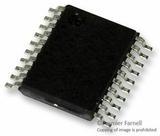
20-lead, RoHS-compliant TSSOP and LFCSP
APPLICATIONS
Optical transceivers
Base station power amplifiers
Process control (PLC input/output cards)
Industrial automation
Data acquisition systems
GENERAL DESCRIPTION
The AD5671R/AD5675R are low power, octal, 12-/16-bit
buffered voltage output digital-to-analog converters (DACs).
They include a 2.5 V, 2 ppm/°C internal reference (enabled by
default) and a gain select pin giving a full-scale output of 2.5 V
(gain = 1) or 5 V (gain = 2). The devices operate from a single
2.7 V to 5.5 V supply and are guaranteed monotonic by design.
The AD5671R/AD5675R are available in a 20-lead TSSOP and in
a 20-lead LFCSP and incorporate a power-on reset circuit and a
RSTSEL pin that ensures the DAC outputs power up to zero scale
or midscale and remain there until a valid write. The AD5671R/
AD5675R contain a power-down mode, reducing the current
consumption to 1 μA typical while in power-down mode.
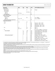
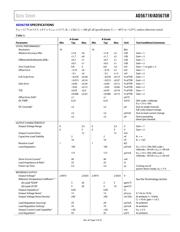
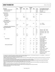
Table 1. Octal nanoDAC+® Devices
Interface Reference 16-Bit 12-Bit
SPI Internal AD5676R AD5672R
External AD5676 Not applicable
I
2
C Internal AD5675R AD5671R
PRODUCT HIGHLIGHTS
1. High Relative Accuracy (INL)
AD5671R (12-bit): ±1 LSB maximum
AD5675R (16-bit): ±3 LSB maximum
2. Low Drift, 2.5 V On-Chip Reference
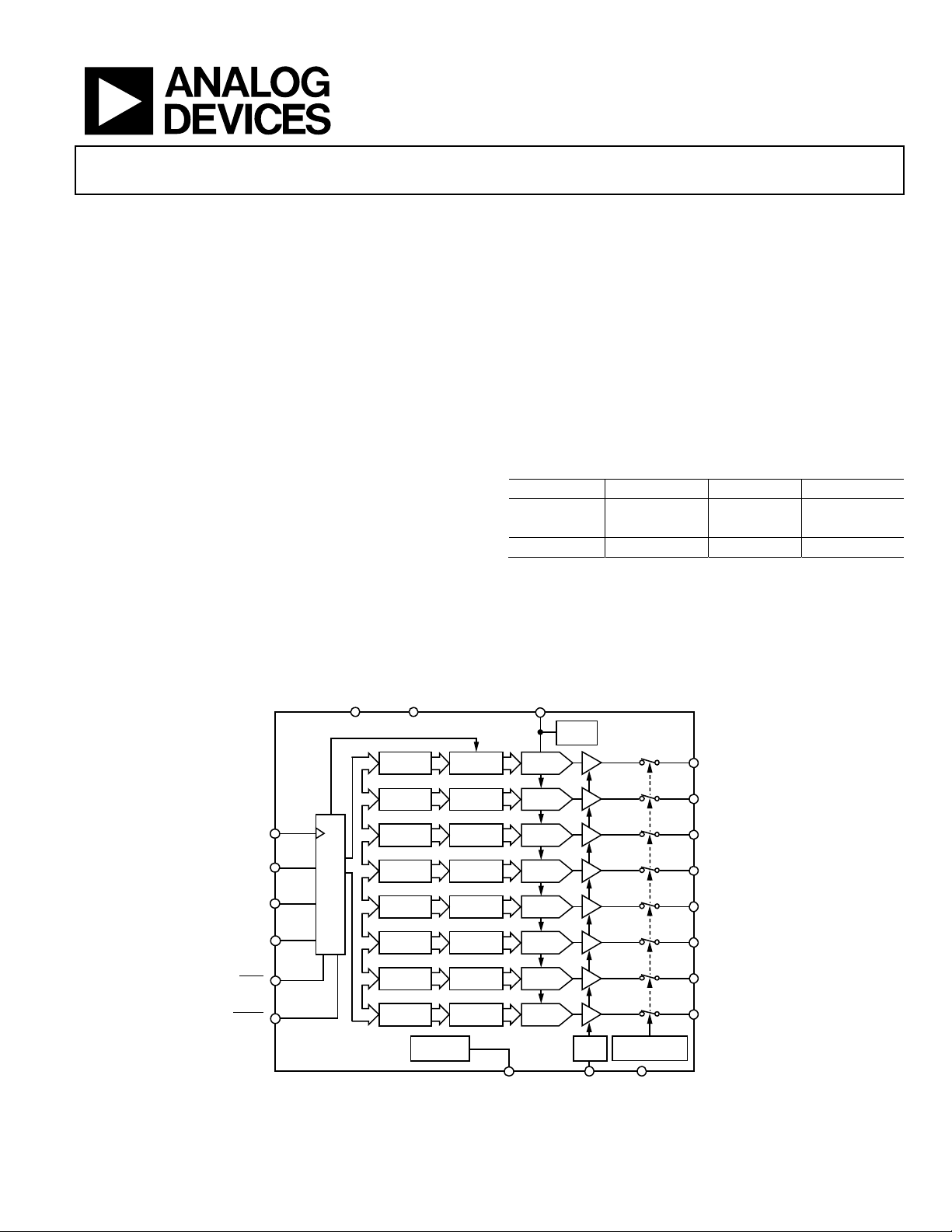
FUNCTIONAL BLOCK DIAGRAM
Figure 1.
INTERFACE LOGIC
INPUT
REGISTER
A0
A1
GND
V
OUT
7
LDAC
SDA
SCL
AD5671R/AD5675R
RESET
2.5V
REF
V
OUT
0
V
OUT
1
V
OUT
2
V
OUT
3
V
OUT
4
V
OUT
5
V
OUT
6
DAC
REGISTER
STRING
DAC 0
BUFFER
INPUT
REGISTER
DAC
REGISTER
STRING
DAC 1
BUFFER
INPUT
REGISTER
DAC
REGISTER
STRING
DAC 2
BUFFER
INPUT
REGISTER
DAC
REGISTER
STRING
DAC 3
BUFFER
INPUT
REGISTER
DAC
REGISTER
STRING
DAC 4
BUFFER
INPUT
REGISTER
DAC
REGISTER
STRING
DAC 5
BUFFER
INPUT
REGISTER
DAC
REGISTER
STRING
DAC 6
BUFFER
INPUT
REGISTER
DAC
REGISTER
STRING
DAC 7
BUFFER
GAIN
POWER-DOWN
LOGIC
POWER-ON
RESET
V
LOGIC
V
DD
V
REFOUT
RSTSEL
GAIN
×1/×2
12664-001
页面指南