

下载
Keywords:
PCB design, PCB design layout, PCB checklist, quad flat pack, quad flat package, QFN assembly, QFN fabrication
APPLICATION NOTE 5963
SMT ASSEMBLY AND PCB DESIGN GUIDELINES FOR MAXIM’S
FLIP-CHIP EXPOSED DIE QFN (NO LEADS) PACKAGES
By:
Phil Eisenberg
Abstract: This document provides a checklist of the critical items to observe during PCB design and layout for systems using Maxim's flip-chip
exposed die QFN packages. The objective is to ensure that projects operate successfully at initial power-up.
Introduction
The QFN or Quad Flat package No leads is an industry standard in plastic molded packages.
QFN packages have the following advantages:
Small footprint per I/O resulting in significant PCB space savings.
Superior electrical and thermal performance compared to leaded plastic packages.
Utilizes standard surface mount assembly technology.
Proven Board-Level Reliability (BLR) per IPC-9701 standards.
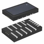
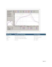
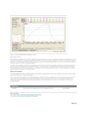
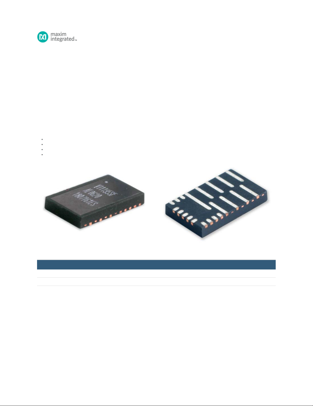
Figure 1a. QFN Isometric Top View. Figure 1b. QFN Isometric Bottom View.
Table 1. Key Attributes for Maxim QFN Packages
Typical Lead Pitch Control 0.5mm/Power 1.0mm
Package Total Height 0.95mm
Lead Coplanarity Leadless
Moisture Sensitivity Classification MSL 1 2 Depending on Package Size
QFN Transportation Media
The QFN is shipped in standard polycarbonate conductive carrier tape with pressure-sensitive adhesive cover tape.
The tape and reel is sealed inside an ESD bag. A flat cardboard box is used to store the sealed bag with the appropriate label.
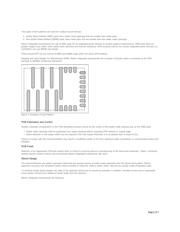
PCB Pad Design
A well-designed and manufactured printed circuit board (PCB) is required for optimum manufacturing yields and product performance.
Page 1 of 7