


下载
APPLICATION NOTE
PRACTICAL CONSIDERATIONS IN HIGH PERFORMANCE
MOSFET, IGBT and MCT GATE DRIVE CIRCUITS
BILL ANDREYCAK
U-137
INTRODUCTION
The switchmode power supply industry’s trend towards higher conversion frequencies is justified by the
dramatic improvement in obtaining higher power densities. And as these frequencies are pushed towards
and beyond one megahertz, the Mosfet transition periods can become a significant portion of the total
switching period. Losses associated with the overlap of switch voltage and current not only degrade the
overall power supply efficiency, but warrant consideration from both a thermal and packaging standpoint.
A/though brief, each of the Mosfet switching transitions can be further reduced if driven from from a high
speed, high current totem-pole driver - one designed exclusively for this application. This paper will highlight
three such devices; the UC1708 and UC1710 high current Mosfet driver ICs, and the UC1711 high speed
driver. Other Mosfet driver ICs and typical application circuits are featured in UNITRODE Application Note
U-118.
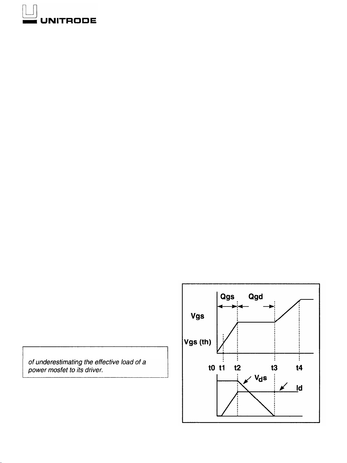
EFFECTIVE GATE CAPACITANCE
The Mosfet input capacitance (Ciss) is frequently
misused as the load represented by a power mosfet
to the gate driver IC. In reality, the effective input
capacitance of a Mosfet (Ceff) is much higher, and
must be derived from the manufacturers’ published
total gate charge (Qg) information. Even the speci-
fied maximum values of the gate charge parameter
do not accurately reflect the driver’s instantaneous
loads during a given switching transition. Fortunately,
FET manufacturers provide a curve for the gate-to-
source voltage (Vgs) versus total gate charge in
their datasheets. This will be segmented into four
time intervals of interest per switching transition.
Each of these will be analyzed to determine the
effective gate capacitance and driver requirements
for optimal performance.
Inadequate gate drive is generally the result
TOTAL GATE CHARGE (Qg)
First, a typical high power Mosfet “Gate Charge
versus Gate-to-Source Voltage” curve will be ex-
amined. An IRFP460 device has been selected and
this curve is applicable to most other Fet devices by
adjusting the gate charge numbers accordingly.
Both turn-on and turn-off trasnsitions are shown with
the respective drain currents and drain-to-source
voltages.
TURN-ON WAVEFORMS
Gate voltage vs time
Figure 1.
3-314