
下载

Application Report
SLAA285A – December 2005 – Revised February 2006
Using ADS8411 in a Multiplexed Analog Input Application
Bhaskar Goswami, Rajiv Mantri ........................................................................ Data Acquisition Products
ABSTRACT
This application report is intended as a guide for using an analog multiplexer to
multiplex several input signals to a single high-resolution, high-speed SAR
analog-to-digital converter (ADC). The ADC and the multiplexer used were the
ADS8411 and the TS5A3159/3359, respectively. This document discusses the
important parameters of a multiplexer and defines a few important measurements for
evaluating a multiplexed system. The results of the evaluation are presented.
Contents
1 Introduction .......................................................................................... 2
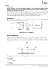
2 Block Diagram ...................................................................................... 2
3 Selection of Multiplexer ............................................................................ 2
4 Input Source ......................................................................................... 3
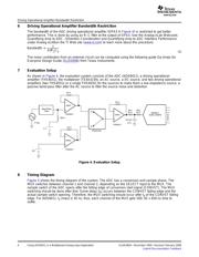
5 Driving Amplifier .................................................................................... 3
6 Driving Operational Amplifier Bandwidth Restriction ........................................... 4
7 Evaluation Setup .................................................................................... 4
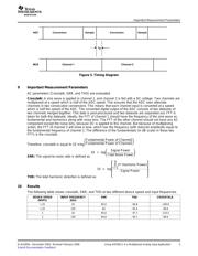
8 Timing Diagram ..................................................................................... 4
9 Important Measurement Parameters ............................................................. 5
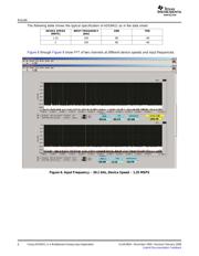
10 Results ............................................................................................... 5
11 Effect of Bandwidth ................................................................................. 9
12 Conclusion ......................................................................................... 11
List of Figures
1 Simplified Block Diagram .......................................................................... 2
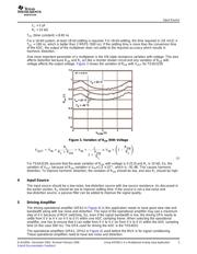
2 Multiplexer Equivalent Circuit ..................................................................... 2
3 Variation of R
ON
With Voltage ..................................................................... 3
4 Evaluation Setup .................................................................................... 4
5 Timing Diagram ..................................................................................... 5
6 Input Frequency – 20.1 kHz, Device Speed – 1.25 MSPS ................................... 6
7 Input Frequency – 101.1 kHz, Device Speed – 1.25 MSPS .................................. 7
8 Input Frequency – 20.1 kHz, Device Speed – 2 MSPS ....................................... 8
9 Input Frequency – 101.1 kHz, Device Speed – 2 MSPS ...................................... 9
10 SNR Versus Input Bandwidth ................................................................... 10
11 Crosstalk Versus Input Bandwidth .............................................................. 10
12 Input Settling With Different Values of Capacitor ............................................. 11
SLAA285A – December 2005 – Revised February 2006 Using ADS8411 in a Multiplexed Analog Input Application 1
Submit Documentation Feedback