
下载
TPS62730
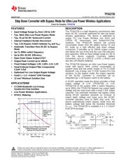
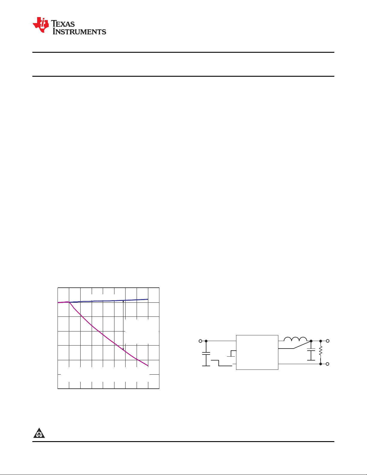
VIN
ON/BYP
STAT
GND
VOUT
SW
V
2.1V
OUT
V
2.2V - 3.9V*
IN
C
2.2
IN
µF
C
2.2
OUT
µF
L 2.2 Hm
ON
BYP
* At V < 2.2V, V tracks V
IN OUT IN
R
pullup
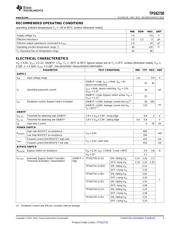
I With TPS62730
BAT
15
17
19
21
23
25
27
29
2 2.2 2.4 2.6 2.8 3 3.2 3.4 3.6 3.8
Battery Voltage - V
BAT
Battery Current
Reduction @
CC2540
0dBm CW TX
Power
Battery Current Reduction of CC2540
2.4GHz Bluetooth Low Energy
System-On-Chip Solution
Battery Current - mA
I NO TPS62730
BAT
TPS62730
www.ti.com
SLVSAC3A –MAY 2011–REVISED MARCH 2012
Step Down Converter with Bypass Mode for Ultra Low Power Wireless Applications
Check for Samples: TPS62730
1
FEATURES
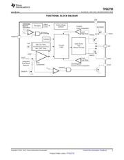
DESCRIPTION
The TPS62730 is a high frequency synchronous step
• Input Voltage Range V
IN
from 1.9V to 3.9V
down DC-DC converter optimized for ultra low power
• Typ. 30nA Ultra Low Power Bypass Mode
wireless applications. The device is optimized to
• Typ. 25 μA DC/DC Quiescent Current
supply TI's Low Power Wireless sub 1GHz and
2.4GHz RF transceivers and System-On-Chip-
• Internal Feedback Divider Disconnect
solutions. The TPS62730 reduces the current
• Typ. 2.1Ω Bypass Switch between V
IN
and V
OUT
consumption drawn from the battery during TX and
• Automatic Transition from DC/DC to Bypass
RX mode by a high efficient step down voltage
Mode
conversion. It provides up to 100mA output current
and allows the use of tiny and low cost chip inductors
• Up To 3MHz switch frequency
and capacitors. With an input voltage range of 1.9V to
• Up to 95% DC/DC Efficiency
3.9V the device supports Li-primary battery
• Open Drain Status Output STAT
chemistries such as Li-SOCl2, Li-SO2, Li-MnO2 and
also two cell alkaline batteries.
• Output Peak Current up to 100mA
• Fixed Output Voltages 1.9V, 2.05V, 2.1V, 2.3V
The TPS62730 features an Ultra Low Power bypass
mode with typical 30nA current consumption to
• Small External Output Filter Components
support sleep and low power modes of TI's CC2540
2.2μH/ 2.2μF
Bluetooth Low Energy and CC430 System-On-Chip
• Optimized For Low Output Ripple Voltage
solutions. In this bypass mode, the output capacitor
• Small 1 × 1.5 × 0.6mm
3
SON Package
of the DC/DC converter is connected via an
integrated typ. 2.1Ω Bypass switch to the battery.
• 12 mm
2
Minimum Solution Size
In DC/DC operation mode the device provides a fixed
APPLICATIONS
output voltage of 2.1V (TPS62730) or 2.3V
(TPS62733) to the system. With a switch frequency
• CC2540 Bluetooth Low Energy
up to 3MHz, the TPS62730 features low output ripple
System-On-Chip Solution
voltage and low noise even with a small 2.2uF output
• Low Power Wireless Applications
capacitor. The automatic transition into bypass mode
during DC/DC operation prevents an increase of
• RF4CE, Metering
output ripple voltage and noise once the DC/DC
converter operates close to 100% duty cycle. The
device automatically enters bypass mode once the
battery voltage falls below the transition threshold
V
IT BYP
. The TPS62730 is available in a 1 × 1.5mm
2
6 pin QFN package.
1
Please be aware that an important notice concerning availability, standard warranty, and use in critical applications of
Texas Instruments semiconductor products and disclaimers thereto appears at the end of this data sheet.
PRODUCTION DATA information is current as of publication date.
Copyright © 2011–2012, Texas Instruments Incorporated
Products conform to specifications per the terms of the Texas
Instruments standard warranty. Production processing does not
necessarily include testing of all parameters.