
下载
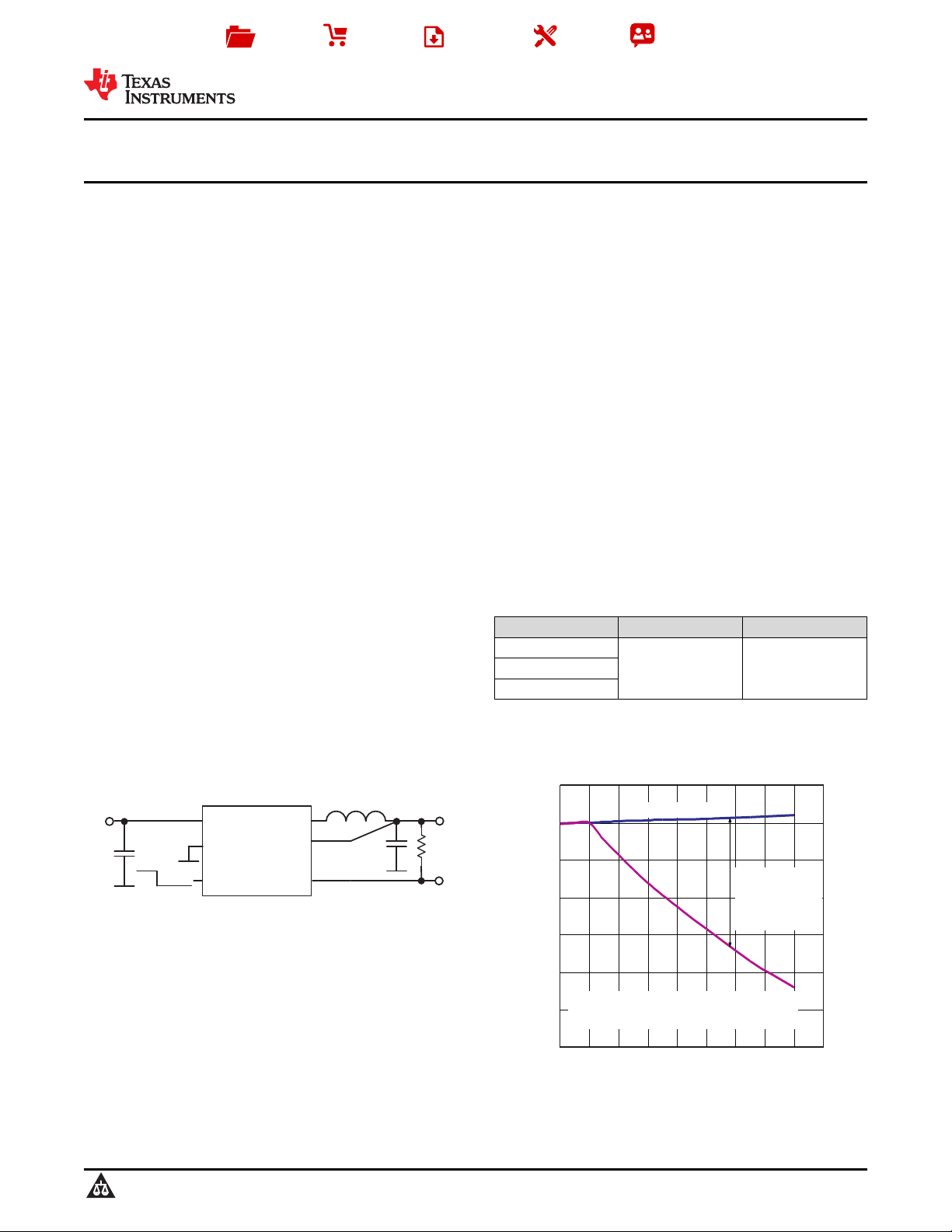
I With TPS62730
BAT
15
17
19
21
23
25
27
29
2 2.2 2.4 2.6 2.8 3 3.2 3.4 3.6 3.8
Battery Voltage - V
BAT
Battery Current
Reduction @
CC2540
0dBm CW TX
Power
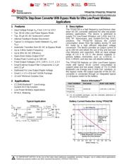
Battery Current Reduction of CC2540
2.4GHz Bluetooth Low Energy
System-On-Chip Solution
Battery Current - mA
I NO TPS62730
BAT
TPS62730
VIN
ON/BYP
STAT
GND
VOUT
SW
V
2.1V
OUT
V
2.2V - 3.9V*
IN
C
2.2
IN
µF
C
2.2
OUT
µF
L 2.2 Hm
ON
BYP
* At V < 2.2V, V tracks V
IN OUT IN
R
pullup
Product
Folder
Sample &
Buy
Technical
Documents
Tools &
Software
Support &
Community
TPS62730
,
TPS62732
,
TPS62733
SLVSAC3D –MAY 2011–REVISED DECEMBER 2014
TPS6273x Step-Down Converter With Bypass Mode for Ultra Low-Power Wireless
Applications
1 Features 3 Description
The TPS62730 is a high frequency synchronous step-
1
• Input Voltage Range V
IN
From 1.9 V to 3.9 V
down DC-DC converter optimized for ultra low-power
• Typ. 30-nA Ultra Low-Power Bypass Mode
wireless applications. The device is optimized to
• Typ. 25-μA DC-DC Quiescent Current
supply TI's Low-Power Wireless sub 1-GHz and 2.4-
GHz RF transceivers and System-On-Chip (SoC)
• Internal Feedback Divider Disconnect
solutions. The TPS62730 reduces the current
• Typical 2.1-Ω Bypass Switch Between V
IN
and
consumption drawn from the battery during TX and
V
OUT
RX mode by a high efficient step-down voltage
• Automatic Transition from DC-DC to Bypass Mode
conversion. The device provides an output current of
up to 100 mA and allows the use of tiny and low-cost
• Up to 3-MHz Switch Frequency
chip inductors and capacitors. With an input voltage
• Up to 95% DC-DC Efficiency
range of 1.9 V to 3.9 V, the device supports Li-
• Open-Drain Status Output STAT
primary battery chemistries such as Li-SOCl2, Li-
• Output Peak Current up to 100 mA
SO2, Li-MnO2, and also two cell alkaline batteries.
• Fixed Output Voltages 1.9 V, 2.05 V, 2.1 V, 2.3 V
The TPS62730 features an Ultra Low-Power bypass
mode with typical 30-nA current consumption to
• Small External Output Filter Components 2.2 μH
support sleep and low power modes of TI's CC2540
and 2.2 μF
Bluetooth Low Energy and CC430 SoC solutions. In
• Optimized For Low Output Ripple Voltage
this bypass mode, the output capacitor of the DC-DC
• Small 1 × 1.5 × 0.6-mm
3
USON Package
converter is connected through an integrated typical
• 12-mm
2
Minimum Solution Size
2.1-Ω bypass switch to the battery.
Device Information
(1)
2 Applications
PART NUMBER PACKAGE BODY SIZE (NOM)
• CC2540 Bluetooth™ Low-Energy
TPS62730
System-On-Chip Solution
TPS62732 USON (6) 1.45 mm x 1.00 mm
• Low-Power Wireless Applications
TPS62733
• RF4CE, Metering
(1) For all available packages, see the orderable addendum at
the end of the datasheet.
Typical Application Battery Current Reduction Using TPS62730
1
An IMPORTANT NOTICE at the end of this data sheet addresses availability, warranty, changes, use in safety-critical applications,
intellectual property matters and other important disclaimers. PRODUCTION DATA.
页面指南