

下载
1
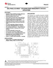
FEATURES
DESCRIPTION
APPLICATIONS
1
2
3
4
DROOP
VREF
GND
CSP1
TPS51727
RHA
5
6
7
8
CSN1
CSN2
CSP2
PGND
V5FILT
ISLEW
OSRSEL
TONSEL
TRIPSEL
PMON
40 39 38 37 36 35 34 33
30
29
28
27
26
25
23
22
DRVH1
VBST
LL1
DRVL1
V5IN
PGND
DRVL2
LL2
L1
0.36 mH
C4
C11
1 mF
THAL
V
OUT
C1
1 mF
R5
R1
PGOOD
UDG-08003
VBAT
9
10
C8
GFB
VFB
THRM
R
T2
R6
VFB
R7
CSP1
CSN1
CSN2
CSP2
GFB
C6
VREF
EN
32 31
SLP
24
21
11 12 13 14 15 16 17 18 19 20
PCNT
PD1
VID4
VID3
VID2
VID1
VID0
DACS
VBST2
DRVH2
C
IN
C
OUT
+
L2
0.36 mH
Time Constant
and
Thermal Matching
CSP2
CSN2
C10
1 mF
PGND
Q4
THAL
VID4
VID3
VID2
VID1
VID0
PD2
Q1
Q2
Q3
VBAT
VREF
V5
V5
PMON
PGOOD
EN
SLP
Time Constant
and
Thermal Matching
CSP1
CSN1
N/C
PCNT
V5
V
OUT
TPS51727
www.ti.com
..................................................................................................................................................... SLUS806B – APRIL 2008 – REVISED JANUARY 2009
DUAL-PHASE, ECO-MODE™ STEP-DOWN POWER MANAGEMENT IC FOR 50-A+
APPLICATIONS
2
• Seamless Phase Add/Drop Enables Maximum
Efficiency Under Any Load Condition
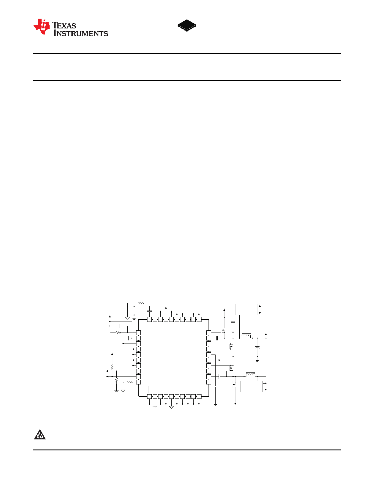
The TPS51727 is a complete, step down controller
with integrated gate drivers. The PCNT pin enables
• Minimum External Parts Count
operation in dual or single-phase mode to optimize
• ± 8 mV VOUT Accuracy Over Line/Load/Temp.
efficiency depending on the load requirements. The
• 5-Bit DAC with 0.4-V to 1.25-V Output Range
advanced D-CAP+™ architecture provides fast
Supports Wide Range of Applications
transient response with minimum output capacitance.
The DAC supports VID-on-the-fly transitions to
• Optimized Efficiency at Light & Heavy Loads
optimize the output voltage to the operating state of
• Patent Pending Output Overshoot Reduction
the system to meet idle power requirements. The
( OSR™)
auto-skip feature of the TPS51727 optimizes
• Accurate, Adjustable Voltage Positioning
light-load efficiency in both single and dual phase
operation. System management features include an
• Selectable 200/300/400/500 kHz Frequency
adjustable thermal sensor, output power monitoring
• Pat. pending AutoBalance™ Phase Balancing
and sleep state controls. Adjustable control of VOUT
• Supports Resistor or Inductor DCR Current
slew rate and voltage positioning are provided. In
Sensing
addition, the TPS51727 includes two high-current
MOSFET gate drivers to drive high and low side
• Accurate, Selectable Current Limit
N-channel MOSFETs with exceptionally high speed
• 4.5-V to 28-V Conversion Voltage Range
and low switching loss The PCNT and VID0 through
• Fast MOSFET Driver w/Integrated Boost Diode
VID4, pins have flexible LV I/O thresholds that enable
interface with logic voltages from 1.0 V to 3.6 V. The
• Integrated OVP Can Be Disabled Thermal
TPS51727 is packaged in a space saving, thermally
Sensor and Output Power Monitor
enhanced, RoHS compliant 40-pin QFN and is rated
• Small 6 × 6, 40-Pin QFN PowerPAD™ Package
to operate from – 10 ° C to 100 ° C.
• High-Current, Low-Voltage Applications for
Adapter, Battery, NVDC or 5-V/12-V Rails
1
Please be aware that an important notice concerning availability, standard warranty, and use in critical applications of Texas
Instruments semiconductor products and disclaimers thereto appears at the end of this data sheet.
2 ECO-MODE, OSR, AutoBalance, PowerPAD, D-CAP+, D-CAP+ are trademarks of Texas Instruments.
PRODUCTION DATA information is current as of publication date.
Copyright © 2008 – 2009, Texas Instruments Incorporated
Products conform to specifications per the terms of the Texas
Instruments standard warranty. Production processing does not
necessarily include testing of all parameters.