
下载

1
SLVA771–June 2016
Submit Documentation Feedback
Copyright © 2016, Texas Instruments Incorporated
Fundamentals of On-Resistance in Load Switches
Application Report
SLVA771–June 2016
Fundamentals of On-Resistance in Load Switches
Joshua Fu............................................................................................................. High Volume Linear
ABSTRACT
Two key concerns for any electrical system are power dissipation and proper voltage regulation. However,
inherent and parasitic resistances create challenges for both. This application report discusses the
fundamentals of load switch On-resistance and how to select a load switch with the right On-resistance
depending on the system requirements.
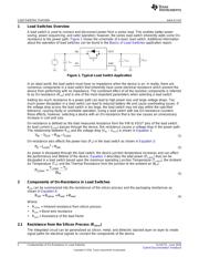
Contents
1 Load Switches Overview.................................................................................................... 2
2 Components of On-Resistance in Load Switches....................................................................... 2
2.1 Resistance from the Silicon Process (R
silicon
) .................................................................... 2
2.2 Bond Wire Resistance (R
wire
) ...................................................................................... 3
2.3 Lead Frame Resistance (R
lead
) .................................................................................... 4
3 Factors that Affect On-Resistance......................................................................................... 4
3.1 Effects of Load Current on On-Resistance...................................................................... 4
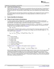
3.2 Effect of Temperature on On-Resistance........................................................................ 5
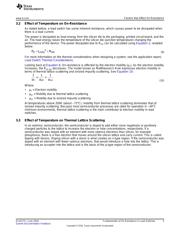
3.3 Effect of Temperature on Thermal Lattice Scattering.......................................................... 5
3.4 Effects of Supply Voltage on On-Resistance ................................................................... 7
4 On-Resistance Applications Examples ................................................................................... 8
5 Conclusion.................................................................................................................... 8
List of Figures
1 Typical Load Switch Application........................................................................................... 2
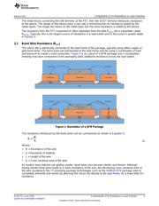
2 Illustration of a QFN Package.............................................................................................. 3
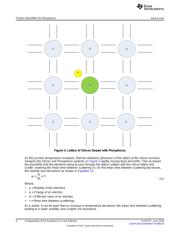
3 Lattice of Silicon Doped with Phosphorus................................................................................ 6
4 Block Diagram of Load Switch without VBIAS Pin ...................................................................... 7
5 Block Diagram of Load Switch with VBIAS Pin.......................................................................... 7