
下载
Semiconductor Components Industries, LLC, 2005
February, 2005 − Rev. 1
1 Publication Order Number:
AND8159/D
AND8159/D
Applications for
Compandors NE570/SA571
Applications
The following circuits will illustrate some of the wide
variety of applications for the NE570/SA571.
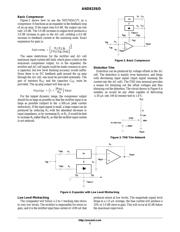
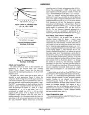
Basic Expandor
Figure 1 shows how the circuit would be hooked up for
use as an expandor. Both the rectifier and G cell inputs are
tied to V
IN
so that the gain is proportional to the average
value of (V
IN
). Thus, when V
IN
falls 6.0 dB, the gain drops
6.0 dB and the output drops 12 dB. The exact expression for
the gain is:
Gain exp.
2R
3
V
IN
(avg)
R
1
R
2
I
B
2
I
B
140 A
The maximum input that can be handled by the circuit
in Figure 1 is a peak of 3.0 V. The rectifier input current
can be as large as I = 3.0 V/R
1
= 3.0 V/10 k = 300 A.
The G cell input current should be limited to
I = 2.8 V/R
2
= 2.8 V/20 k = 140 A. If it is necessary to
handle larger input voltages than 0 2.8 V peak, external
resistors should be placed in series with R
1
and R
2
to limit
the input current to the above values.
Figure 1 shows a pair of input capacitors C
IN1
and C
IN2
.
It is not necessary to use both capacitors if low level tracking
accuracy is not important. If R
1
and R
2
are tied together and
share a common capacitor, a small current will flow between
the G cell summing node and the rectifier summing node
due to offset voltages. This current will produce an error in
the gain control signal at low levels, degrading tracking
accuracy.
Figure 1. Basic Expandor
V
IN
V
OUT
R
3
R
2
R
1
C
IN1
C
IN2
C
RECT
R
4
∆G
V
REF
−
+
The output of the expandor is biased up to 3.0 V by the DC
gain provided by R
3
, R
4
. The output will bias up to:
V
OUTDC
1
R
3
R
4
V
REF
For supply voltages higher than 6.0 V, R
4
can be shunted
with an external resistor to bias the output up to V
CC
.
Note that it is possible to externally increase R
1
, R
2
, and
R
3
, and to decrease R
3
and R
4
. This allows a great deal of
flexibility in setting up system levels. If larger input signals
are to be handled, R
1
and R
2
may be increased; if a larger
output is required, R
3
may be increased. To obtain the largest
dynamic range out of this circuit, the rectifier input should
always be as large as possible (subject to the 300 A peak
current restriction).
APPLICATION NOTE
http://onsemi.com