
下载

Comparison between
MM912_634 and
MC9S12VR Family
by: NXP Semiconductors
1 Introduction
The objective of this application note is to provide a comparison between
these three MCUs, MM912_634, MC9S12VR, and MC9S12VRP. For more
detailed information, please review the reference manual.
The following modules and functionalities are compared in this document:
• Clock, Reset and Power Management Unit
• Interrupt Module
• Debug Module
• Current Sense Amplifier Module
• Voltage Regulator
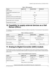
• Analog-to-Digital Converter Module
• Pulse-Width-Modulation Module
• Capability to supply external devices as a Hall Sensor
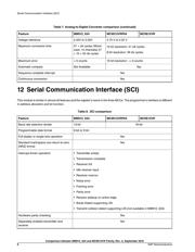
• Serial Communication Interface
• High-Side Drivers
• Low-Side Drivers
• LIN Physical Layer
• High Voltage Inputs
• Timer Module
• Battery Sense Module
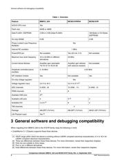
2 Overview
These three MCU can be used in relay-driven motor control applications. The following table presents a quick comparison
of the main differences between MM12_634, MC9S12VRP, and MC9S12VR. The complete comparison of these modules
are described in subsequent sections.
Contents
1 Introduction........................................... 1
2 Overview................................................ 1
3 General software and debugging
compatibility........................................2
4 Clock, Reset, and Power
Management Unit (CPMU)..................3
5 Interrupt Module (INT)...........................3
6 Debug Module (DBG)............................ 3
7 Voltage Regulator (VREG).................... 3
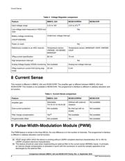
8 Current Sense........................................4
9 Pulse-Width-Modulation Module
(PWM)...................................................4
10 Capability to supply external
devices as a Hall Sensor (HALL).......5
11 Analog-to-Digital Converter
(ADC) module .....................................5
12 Serial Communication Interface
(SCI)..................................................... 6
13 High-Side Drivers (HSD)..................... 7
14 High Voltage Inputs (HVI)................... 7
15 Low-Side Drivers (LSD).......................8
16 LIN Physical Layer (LIN PHY)............. 8
17 Timer Module (TIM)..............................9
18 Battery Sense Module......................... 9
19 Package Pinout comparison.............10
20 Revision history.................................11
NXP Semiconductors
Document Number: AN5328
Application Note Rev. 0, September 2016