
下载
© Semiconductor Components Industries, LLC, 2013
August, 2013 − Rev. 9
1 Publication Order Number:
PZT2222AT1/D
PZT2222A
NPN Silicon Planar
Epitaxial Transistor
This NPN Silicon Epitaxial transistor is designed for use in linear
and switching applications. The device is housed in the SOT−223
package which is designed for medium power surface mount
applications.
Features
• PNP Complement is PZT2907AT1
• The SOT−223 Package Can be Soldered Using Wave or Reflow
• SOT−223 Package Ensures Level Mounting, Resulting in Improved
Thermal Conduction, and Allows Visual Inspection of Soldered
Joints
• The Formed Leads Absorb Thermal Stress During Soldering,
Eliminating the Possibility of Damage to the Die
• Available in 12 mm Tape and Reel
• S Prefix for Automotive and Other Applications Requiring Unique
Site and Control Change Requirements; AEC−Q101 Qualified and
PPAP Capable
• These Devices are Pb−Free, Halogen Free/BFR Free and are RoHS
Compliant*
MAXIMUM RATINGS
Rating Symbol Value Unit
Collector−Emitter Voltage V
CEO
40 Vdc
Collector−Base Voltage V
CBO
75 Vdc
Emitter−Base Voltage
(Open Collector)
V
EBO
6.0 Vdc
Collector Current I
C
600 mAdc
Total Power Dissipation
up to T
A
= 25°C (Note 1)
P
D
1.5
W
Storage Temperature Range° T
stg
− 65 to +150 °C
Junction Temperature° T
J
150 °C
Stresses exceeding Maximum Ratings may damage the device. Maximum
Ratings are stress ratings only. Functional operation above the Recommended
Operating Conditions is not implied. Extended exposure to stresses above the
Recommended Operating Conditions may affect device reliability.
1. Device mounted on an epoxy printed circuit board 1.575 inches x 1.575 inches x
0.059 inches; mounting pad for the collector lead min. 0.93 inches
2
.
THERMAL CHARACTERISTICS
Rating Symbol Value Unit
Thermal Resistance,
Junction−to−Ambient
R
q
JA
83.3 °C/W
Lead Temperature for Soldering,
0.0625″ from case
Time in Solder Bath
T
L
260
10
°C
Sec
*For additional information on our Pb−Free strategy and soldering details, please download the ON Semiconductor Soldering and Mounting
Techniques Reference Manual, SOLDERRM/D.
http://onsemi.com
MARKING DIAGRAM
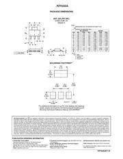
SOT−223 (TO−261)
CASE 318E−04
STYLE 1
Device Package Shipping
†
ORDERING INFORMATION
PZT2222AT1G SOT−223
(Pb−Free)
1,000 Tape & Reel
†For information on tape and reel specifications,
including part orientation and tape sizes, please
refer to our Tape and Reel Packaging Specifications
Brochure, BRD8011/D.
A = Assembly Location
Y = Year
M = Month Code
G = Pb−Free Package
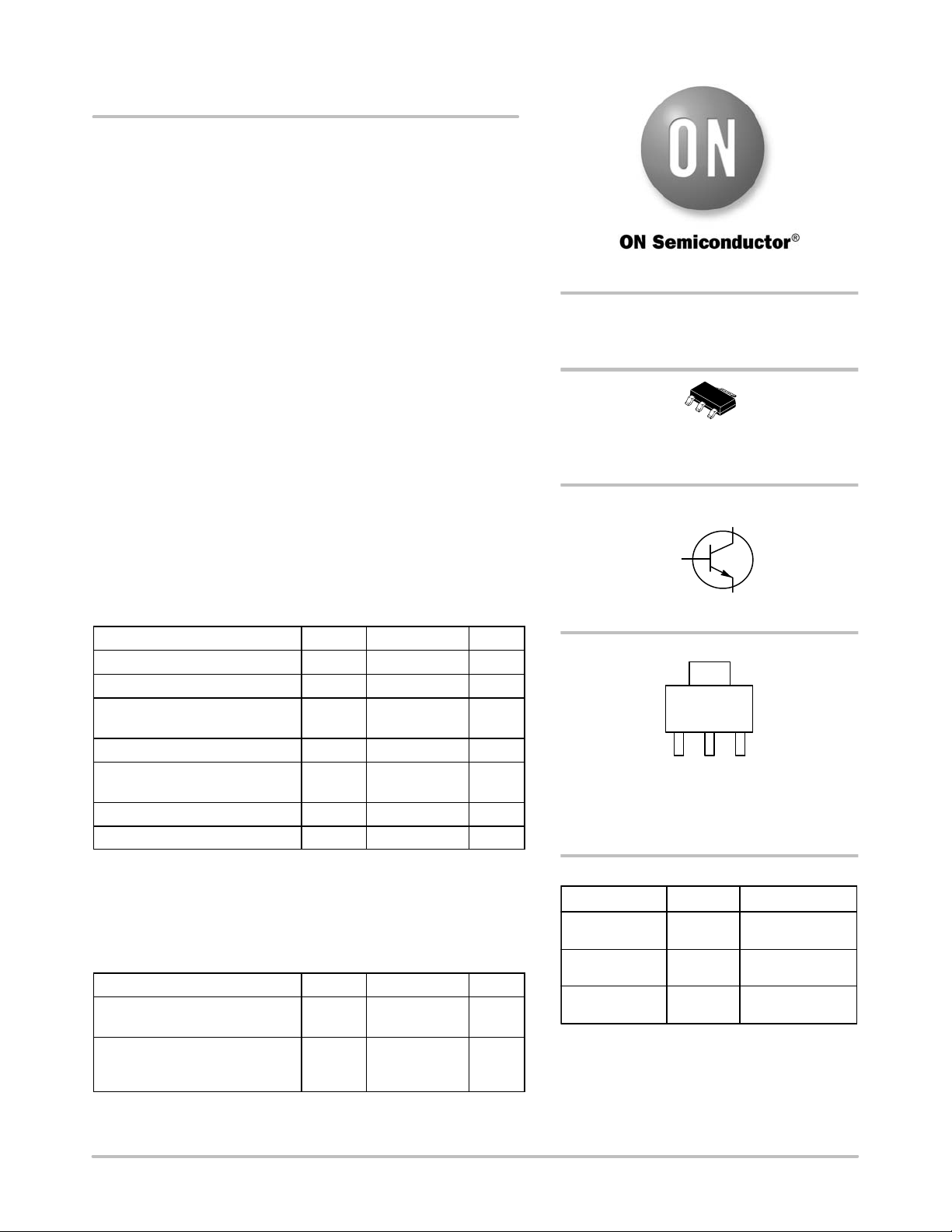
BASE
1
COLLECTOR
2, 4
3
EMITTER
SOT−223 PACKAGE
NPN SILICON TRANSISTOR
SURFACE MOUNT
PZT2222AT3G SOT−223
(Pb−Free)
4,000 Tape & Reel
AYM
P1FG
G
(Note: Microdot may be in either location)
SPZT2222AT1G SOT−223
(Pb−Free)
1,000 Tape & Reel
1
2
3
4