
下载
Semiconductor Components Industries, LLC, 2005
January, 2005 − Rev. 6
1 Publication Order Number:
MGSF1N03LT1/D
MGSF1N03LT1
Preferred Device
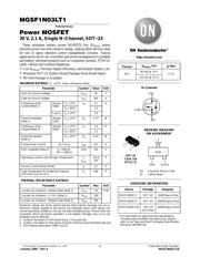
Power MOSFET
30 V, 2.1 A, Single N−Channel, SOT−23
These miniature surface mount MOSFETs low R
DS(on)
assure
minimal power loss and conserve energy, making these devices ideal
for use in space sensitive power management circuitry. Typical
applications are dc−dc converters and power management in portable
and battery−powered products such as computers, printers, PCMCIA
cards, cellular and cordless telephones.
• Low R
DS(on)
Provides Higher Efficiency and Extends Battery Life
• Miniature SOT−23 Surface Mount Package Saves Board Space
• Pb−Free Package is Available
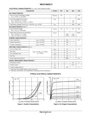
MAXIMUM RATINGS (T
J
= 25°C unless otherwise noted)
Parameter Symbol Value Unit
Drain−to−Source Voltage V
DSS
30 V
Gate−to−Source Voltage V
GS
±20 V
Continuous Drain
Current (Note 1)
Steady
State
T
A
= 25°C
I
D
2.1
A
Current (Note 1) State
T
A
= 85°C 1.5
t ≤ 10 s T
A
= 25°C 2.8
Power Dissipation
(Note 1)
Steady
State
T
A
= 25°C P
D
0.73 W
Continuous Drain
Current (Note 2)
Steady
State
T
A
= 25°C
I
D
1.6
A
Current (Note 2) State
T
A
= 85°C 1.1
Power Dissipation
(Note 2)
T
A
= 25°C P
D
0.42 W
Pulsed Drain Current tp = 10 s I
DM
6.0 A
ESD Capability (Note 3) C = 100 pF,
RS = 1500
ESD 125 V
Operating Junction and Storage Temperature T
J
,
T
STG
−55 to
150
°C
Source Current (Body Diode) I
S
2.1 A
Lead Temperature for Soldering Purposes
(1/8” from case for 10 s)
T
L
260 °C
THERMAL RESISTANCE RATINGS
Parameter Symbol Max Unit
Junction−to−Ambient − Steady State (Note 1) R
JA
170
°C/W
Junction−to−Ambient − t < 10 s (Note 1) R
JA
100
Junction−to−Ambient − Steady State (Note 2) R
JA
300
Maximum ratings are those values beyond which device damage can occur.
Maximum ratings applied to the device are individual stress limit values (not
normal operating conditions) and are not valid simultaneously. If these limits are
exceeded, device functional operation is not implied, damage may occur and
reliability may be affected.
1. Surface−mounted on FR4 board using 1 in sq pad size.
2. Surface−mounted on FR4 board using the minimum recommended pad size.
3. ESD Rating Information: HBM Class 0.
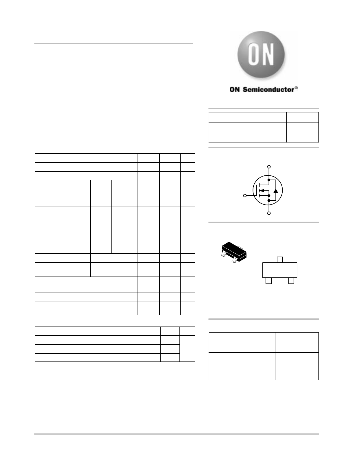
G
D
S
Device Package Shipping
†
ORDERING INFORMATION
MGSF1N03LT1 SOT−23 3000/Tape & Reel
30 V
125 m @ 4.5 V
80 m @ 10 V
R
DS(on)
TYP
2.1 A
I
D
MAXV
(BR)DSS
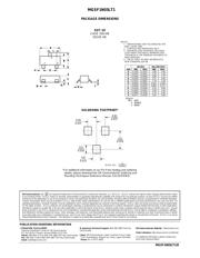
SOT−23
CASE 318
STYLE 21
MARKING DIAGRAM/
PIN ASSIGNMENT
2
N3 = Specific Device Code
W = Work Week
3
N3W
1
3
Drain
1
Gate
2
Source
N−Channel
MGSF1N03LT3 SOT−23 10000/Tape & Reel
†For information on tape and reel specifications,
including part orientation and tape sizes, please
refer to our Tape and Reel Packaging Specification
Brochure, BRD8011/D.
MGSF1N03LT3G SOT−23
(Pb−Free)
10000/Tape & Reel
http://onsemi.com