
下载
Semiconductor Components Industries, LLC, 2005
June, 2005 − Rev. 1
1 Publication Order Number:
AND8200/D
AND8200/D
Design Considerations for
ESD/EMI Filters: I
(Almost Everything You Wanted to Know
About EMI Filters and Were Afraid to Ask)
Prepared by: Ryan Hurley
Applications Engineer
ON Semiconductor
Background
With data transfer rates and clock frequencies ever
increasing and encroaching on radio frequencies, the need
for EMI filters has increased dramatically. At the same time,
the portability of electronic devices such as PDAs, laptop
computers, MP3 players and so on, the need to protect those
devices from ESD has also increased because use of
peripheral interfaces. Some time ago these two functions
were independent of each other with discrete components
making the EMI filter and a separate device to provide the
ESD protection. As consumer electronics continue to get
smaller, the ESD and EMI filter functions were gradually
integrated together.
For ESD protection, a TVS diode would typically be used.
TVS diodes are nothing more than Zener diodes that have
been modified to handle large currents for very brief periods
of time while “clamping” at some voltage slightly over the
peak operating voltage. A TVS diode with a clamping
voltage of 6.0 V would be used in applications where the
maximum operating voltage was 3.3 V. There is a limit
however, to the TVS’s ability to clamp. That is a given TVS
can only dissipate so much power in those short periods of
time. A way to improve this is to increase the size of the
TVS. A larger device can handle more current than a similar
but smaller device, but at a cost, more capacitance.
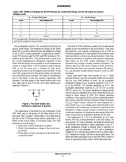
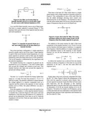
EMI filters have in the past been RC or LC pi networks
using individual surface mount components. One of the
main problems with using discrete components is that there
are parasitics that can negatively affect the performance of
the filter. Overall, most commonly used EMI filters for
portable applications take a form similar to that of Figure 1.
C1 C2
R
Figure 1. Common RC “Pi’’ Filter
These filters are typically low pass filters that reject
signals over 800 MHz. The component values for the filter
are typically determined by how much attenuation is needed
in the rejection band (800 MHz to 2.5 GHz for example), the
source and load impedances, and how much the desired
signal can be attenuated without losing data.
In applications where both ESD and EMI filtering are
required, it is advantageous to choose a single integrated
ESD/EMI filter that replaces a number of discrete surface
mount components. Where board space is a premium, a
single integrated component is hard to beat. If cost is an
issue, a solution composed of a number of discrete surface
mount components cannot compete with a single integrated
ESD/EMI filter. If it is decided that a single integrated
ESD/EMI filter is to be used, a number of questions need to
be answered.
How much ESD protection is required?
What are the EMI filtering requirements?
What is the acceptable Group Delay?
How much insertion loss can be tolerated?
What type of package should be used?
What else?
ESD Protection
How much ESD protection is needed? As much as
possible would be the correct answer. Having too little ESD
has the obvious consequences of inviting damage to
sensitive components that were meant to be protected. Is
there such a thing as too much ESD protection? For high
speed data lines and high frequency lines the answer is
“yes”. The component that does the work for ESD protection
is the TVS or Transient Voltage Suppressor. One of the ways
to measure a TVS’s ability to suppress ESD is in the form of
the IEC 61000−4−2. Level 4 is required for accessible
contacts on cell phones. For further details refer to
AND8074/D.
APPLICATION NOTE
http://onsemi.com