
下载

© Semiconductor Components Industries, LLC, 2002
August, 2016 − Rev. 1
1 Publication Order Number:
AND8104/D
AND8104/D
MicroIntegration Technology
Solutions for Protection in
High Speed I/O Data Lines
INTRODUCTION
Static electricity conditions (ESD) can cause catastrophic
damage to I/O ports, IC malfunction, and worst of all, ghost
data bits in electronic systems. When product damage or
product malfunction results in a “Hard failure” or destroyed
component, it is easy to isolate and replace the failed
component and put the system back in service, however, if
a “soft failure” occurs (CMOS component degraded), the
system anomaly is not detected in retesting, and hours are
wasted in troubleshooting because the system continues to
produce irregular data bits. Such failures have a very
negative impact in the final product because they increase
the cost of warranty repairs and diminish the perception of
the product’s quality.
These days, our modern society has rapidly come to fully
depend on electronics. And modern computers are based
increasingly on low power logic chips, all with ESD
sensitivity due to MOS dielectric breakdowns and bipolar
reverse junction current limits. The ICs that control I/O ports
(USB, Ethernet, etc.) are not an exception since the majority
of them are designed and manufactured based on CMOS
processes which make them extremely sensitive to damage
from ESD conditions. Because the majority of I/O ports are
hot insertion and removal systems, they are extremely
vulnerable to receive ESD conditions possibly generated by
the users or by air discharges. Users can induce ESD
conditions while plugging or unplugging any cables, and air
discharges can happen a few inches away from the
conducting surface.
In addition to all the previous problems caused by static
discharge conditions in unprotected ICs, ESD protection
now is becoming a strong requirement mainly in the
European market, which causes the manufacturers to be
barred from selling in this market unless their
product/equipment meets the minimum levels of ESD
performance. For all these reasons, engineers and designers
must fully understand ESD, which means to be aware of
industry standards, testing methods, voltage and current
waveforms, application circuits, and selection of the right
devices for the protection required in each particular
application.
Electrostatic Discharge Generation
When two insulating materials are rubbed together, an
electric charge builds up between them (as electrons are
stripped off one surface and deposited on the other surface).
The surface with the excess of electrons becomes negatively
charged, and the surface with the shortage of electrons
becomes positively charged. This effect is known as the
“triboelectric” effect (the action of rubbing). Electrostatic
voltage is then a function of the separation of the materials
in the series, the intimacy of contact, and the rate of
separation. Therefore, any time there are two nonconductive
materials flowing in opposition to each other, an
electrostatic voltage will be generated. The level of
electrostatic potential generated depends on the relative
charge affinity between materials, the humidity, and other
factors.
Test Methods for ESD
Two test methods are the most common standards used to
test the ESD susceptibility of integrated circuits. These two
methods are the “Human Body Model (HBM)” and the
“Machine Model (MM)”.
JEDEC developed standards of ESD testing for both the
Human Body Model and Machine Model. These standards
were reviewed and approved by the EIA general counsel.
JEDEC Standard JESD22−A114−B,
Electrostatic Discharge (ESD) Sensitivity Testing
Human Body Model (HBM)
This method establishes a standard procedure for testing
and classifying microcircuits according to their susceptibility
to damage or degradation by exposure to a defined
electrostatic Human Body Model (HBM) discharge (ESD).
The objective is to provide reliable, repeatable HBM ESD test
results so that accurate classifications can be performed.
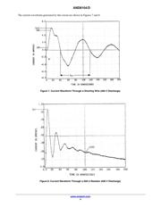
The Human Body Model test method simulates the typical
capacitance and source impedance of a human body. The
resulting current waveform represents the ESD that occurs
when a person touches objects, such as ICs.
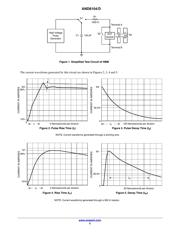
The equivalent circuit for the HBM ESD is shown in
Figure 1, it is basically composed by a high voltage supply,
and an RC network.
APPLICATION NOTE
http://onsemi.com