
下载
© Semiconductor Components Industries, LLC, 2006
April, 2006 − Rev. 6
1 Publication Order Number:
NL27WZ32/D
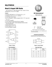
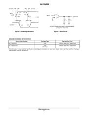
NL27WZ32
Dual 2−Input OR Gate
The NL27WZ32 is a high performance dual 2−input OR Gate
operating from a 1.65 V to 5.5 V supply.
Features
• Extremely High Speed: t
PD
2.5 ns (typical) at V
CC
= 5 V
• Designed for 1.65 V to 5.5 V V
CC
Operation
• Over Voltage Tolerant Inputs
• LVTTL Compatible − Interface Capability With 5 V TTL Logic with
V
CC
= 3 V
• LVCMOS Compatible
• 24 mA Balanced Output Sink and Source Capability
• Near Zero Static Supply Current Substantially Reduces System
Power Requirements
• Replacement for NC7WZ32
• Chip Complexity: FET = 120
• Pb−Free Package is Available
A2
Y2
Figure 1. Pinout
Figure 2. Logic Symbol
w1
Y1
A1
B2
B1
V
CC
A1
B1
GND
1
2
3
8
7
6
4
5
Y2
Y1
B2
A2
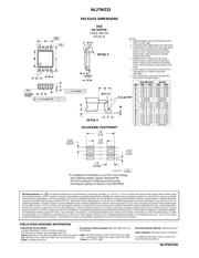
PIN ASSIGNMENT
Pin
1
2
3
4
5
6
7
8
Function
A1
B1
Y2
GND
A2
B2
Y1
V
CC
Input
FUNCTION TABLE
B
L
H
L
H
Output
Y = A + B
Y
L
H
H
H
A
L
L
H
H
IEEE/IEC
See detailed ordering and shipping information in the
package dimensions section on page 4 of this data sheet.
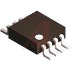
ORDERING INFORMATION
MARKING
DIAGRAM
US8
US SUFFIX
CASE 493
8
1
http://onsemi.com
1
8
L4 M G
G
LR = Device Code
M = Date Code*
G = Pb−Free Package
*Date Code orientation may vary depending upo
n
manufacturing location.
(Note: Microdot may be in either location)