

下载
July 1996
NDS335N
N-Channel Logic Level Enhancement Mode Field Effect Transistor
General Description Features
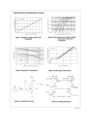
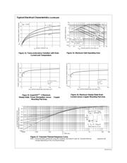
________________________________________________________________________________
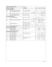
Absolute Maximum Ratings T
A
= 25°C unless otherwise noted
Symbol Parameter NDS335N Units
V
DSS
Drain-Source Voltage 20 V
V
GSS
Gate-Source Voltage - Continuous 8 V
I
D
Maximum Drain Current - Continuous (Note 1a) 1.7 A
- Pulsed 10
P
D
Maximum Power Dissipation (Note 1a) 0.5 W
(Note 1b)
0.46
T
J
,T
STG
Operating and Storage Temperature Range -55 to 150 °C
THERMAL CHARACTERISTICS
R
θ
JA
Thermal Resistance, Junction-to-Ambient
(Note 1a)
250 °C/W
R
θ
JC
Thermal Resistance, Junction-to-Case (Note 1) 75 °C/W
NDS335 Rev.C
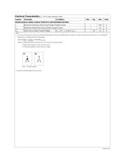
1.7 A, 20 V. R
DS(ON)
= 0.14 Ω @ V
GS
= 2.7 V
R
DS(ON)
= 0.11 Ω @ V
GS
= 4.5 V.
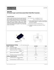
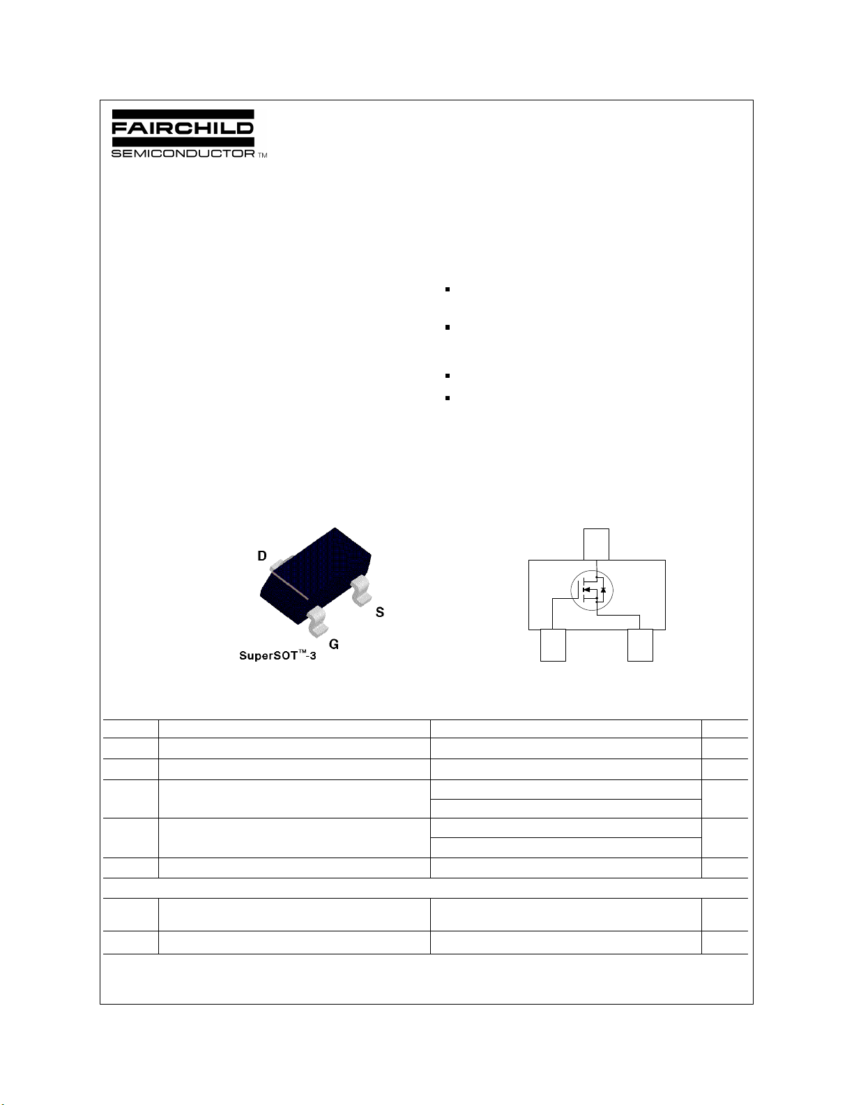
Industry standard outline SOT-23 surface mount package
using poprietary SuperSOT
TM
-3 design for superior thermal
and electrical capabilities.
High density cell design for extremely low R
DS(ON)
.
Exceptional on-resistance and maximum DC current
capability.
These N -Channel logic level enhancement mode power field
effect transistors are produced using Fairchild's proprietary,
high cell density, DMOS technology. This very high density
process is especially tailored to minimize on-state resistance.
These devices are particularly suited for low voltage
applications in notebook computers, portable phones, PCMCIA
cards, and other battery powered circuits where fast switching,
and low in-line power loss are needed in a very small outline
surface mount package.
D
S
G
© 1997 Fairchild Semiconductor Corporation