
下载
Semiconductor Components Industries, LLC, 2000
October, 2000 – Rev. 1
1 Publication Order Number:
AND8031/D
AND8031/D
Isolated Precision
Regulation of a Single
1.8 Volt Output from a
Universal Line Input
Prepared by: Jason Hansen
ON Semiconductor
INTRODUCTION
The following Application Note describes an off–line
switching power supply utilizing a precision programmable
reference to regulate a 1.8 volt output. The center of the app
note is the MC33363B, a monolithic SMPS controller with
a 700 volt power switch, and the NCP100, a sub–one volt
precision programmable reference. The system design and
analysis will be described in detail.
The design requirements are for a universal off–line
converter with a 1.8 volt, 1.0 ampere single output with less
than 50 millivolts ripple and operates at 100 kHz. Most of the
components selected are surface mount. This design is
separated into the generic circuit of the off–line converter
and the feedback network.
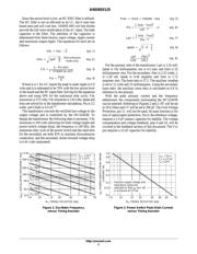
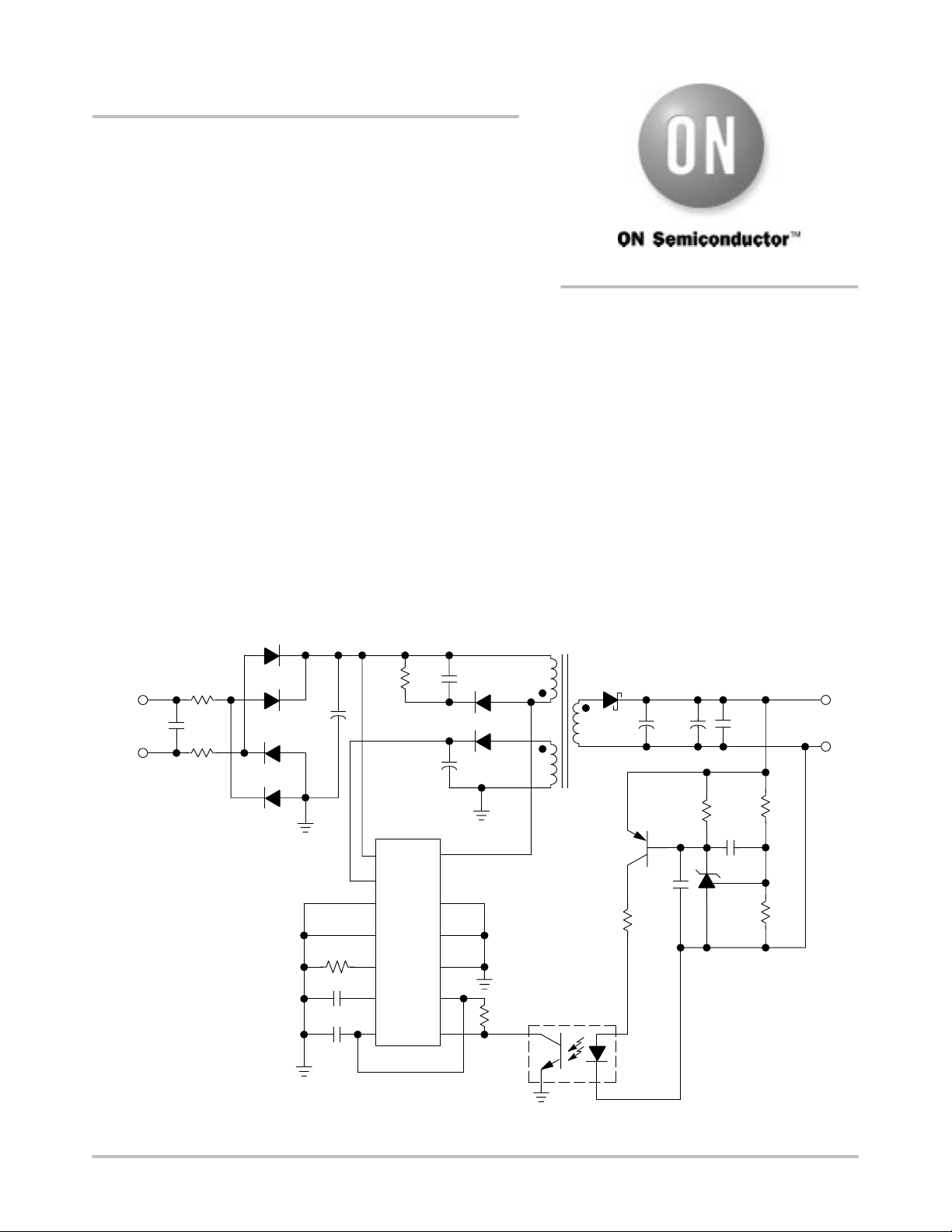
Generic Off–Line Conversion Circuit
To reduce the total number of components and thus
minimize circuit board area, an SMPS controller with an
integrated power switch is selected. With the low output
power requirement, the MC33363B is selected as the control
and power switch IC. The MC33363B contains an externally
programmable frequency and current limit, internal startup
circuit and can handle up to 8 watts of output power.
The basic off–line conversion circuit is illustrated in
Figure 1. The line input is filtered through the EMC circuit
then rectified and filtered. The rectified voltage is converted
to a lower voltage via the transformer and the MC33363B.
The secondary of the transformer is rectified to a DC voltage
and filtered. The output voltage controls the duty cycle of the
switcher via the isolated feedback network. The calculated
values are a starting point and do not replace bench testing.
Figure 1. MC33363B Basic Flyback Circuit Schematic
1
3
4
5
6
7
8
16
13
12
11
10
9
MC33363B
Universal
Input
1N4005
R2
4.7
R1
4.7
C1
1 n
D1
D2
D3
D4
U1
4.7 µ
400 V
R4
3.9 k
C6
10 µ
D6
MURS120
D5
MURS160
C5
47 p
R6
2.7 k
R3 30 k
C3 390 p
C4 1 µ
U3
SFH615–4
C10
1 µ
U4
NCP100
R10
7.5 k
R9
12 k
C9
0.1 µ
R12
120
R11
10
Q1
BC858ALT1
D7
MBRD835L
C7
820 µ
+
–
1.8 V
C8
820 µ
C12
1 µ
U2 CTX22–14966
http://onsemi.com
APPLICATION NOTE