
下载

© Semiconductor Components Industries, LLC, 2007
March, 2007 − Rev. 0
1 Publication Order Number:
AND8278/D
AND8278/D
NCP1351 Evaluation Board
16 V / 32 V – 40 W Printer
Power Supply
Prepared by: Nicolas Cyr
ON Semiconductor
The present document describes a printer power supply
operated by the NCP1351, a fixed t
on
/ variable off time
controller. The board can deliver 10 W average on a 16 V
output and 30 W average on a 32 V output with a transient
peak power capability of 80 W. It however exhibits a low
standby power: below 150 mW at no load whatever the input
voltage. Let us first review the benefit of using the
NCP1351:
The NCP1351 at a Glance
Fixed t
on
, Variable t
off
Current−mode Control:
implementing a fixed peak current mode control (hence the
more appropriate term “quasi−fixed” t
on
), the NCP1351
modulates the off time duration according to the output
power demand. In high power conditions, the switching
frequency increases until a maximum is hit. This upper limit
depends on an external capacitor selected by the designer. In
light load conditions, the off time expands and the NCP1351
operates at a lower frequency. As the frequency reduces, the
contribution of all frequency−dependent losses accordingly
goes down (driver current, drain capacitive losses, switching
losses), naturally improving the efficiency at various load
levels.
Peak Current Compression at Light Loads: Reducing
the frequency will certainly force the converter to operate
into the audible region. To prevent the transformer
mechanical resonance, the NCP1351 gradually reduces –
compresses – the peak current setpoint as the load becomes
lighter. When the current reaches 30% of the nominal value,
the compression stops and the off duration keeps expanding
towards low frequencies.
Low Standby−power: the frequency reduction technique
offers an excellent solution for designers looking for low
standby power converters. Also, compared to the skip−cycle
method, the smooth off time expansion does not bring
additional ripple in no−load conditions: the output voltage
remains quiet.
Natural Frequency Dithering: the quasi−fixed t
on
mode
of operation improves the EMI signature since the switching
frequency varies with the natural bulk ripple voltage.
Extremely Low Start−up Current: built on a
proprietary circuitry, the NCP1351 startup section does not
consume more than 10 mA during the startup sequence. The
designer can thus easily combine startup time and standby
consumption.
Overload Protection Based on Fault Timer: every
designer knows the pain of building converters where a
precise over current limit must be obtained. When the fault
detection relies on the auxiliary V
CC
, the pain even
increases. Here, the NCP1351 observes the lack of feedback
current and starts a timer to countdown. At the end of its
charge, the timer either triggers an auto−recovery sequence
(auto−restart, B and D versions) or permanently latches−off
(A and C). On C and D versions the fault timer is started at
an output power corresponding to 60% of the maximum
deliverable power; to allow transient peak power delivery.
Latch Fault Input: a dedicated input lets the designer
externally trigger the latch to build additional protections
such as over−voltage (OVP) or over−temperature (OTP).
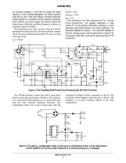
The Schematic
The design must fulfill the following specifications:
Input voltage: 88 – 265 Vac
Output voltage: 16 V @ 0.625 A and 32 V @ 1 A nominal
(40 W); with transient 80 W peak power capability during
40 ms, and 62 W peak during 400 ms
Over power protection below 100 W for the whole input
voltage range (LPS)
Latched short−circuit protection
Latched Over voltage protection
Latch recovery time below 3 s
Brown−out protection
Start−up time below 3 s
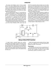
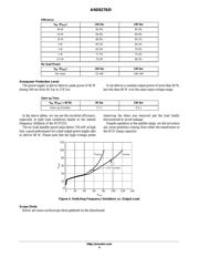
In order to deliver the peak output power, the NCP1351
will increase its switching frequency up to the upper limit set
by the C
T
capacitor. To not jeopardize the EMI test
compliance, the switching frequency should be kept below
150 kHz. We will choose 100 kHz to have a good margin. As
a result the switching frequency at nominal load will be
around 50 kHz. Since we need to deliver 80 W of transient
peak power while ensuring the power will never be above
100 W, we will use the C version of NCP1351, specially
tailored for this kind of application. When the controller
detects a need for a frequency higher than 60 kHz, implying
APPLICATION NOTE
http://onsemi.com