
下载
Semiconductor Components Industries, LLC, 2003
June, 2003 - Rev. 1
1 Publication Order Number:
AND8098/D
AND8098/D
Low−Cost 100 mA
High−Voltage Buck and
Buck−Boost Using NCP1052
Prepared by: Kahou Wong
ON Semiconductor
INTRODUCTION
This application note presents low-cost high-voltage
100 mA non-isolated power supply using NCP1052 by
buck and buck-boost topology. The NCP1052 is one of the
latest low-cost switching controllers with integrated 700 V/
300 mA power switch from ON Semiconductor. It is
primarily designed for isolated 10 W-range flyback
converter. If isolation is not needed, the IC can also be used
as stepping-down buck and buck-boost converter for
further cost saving by removing optocoupler and replacing
the transformer by an inductor. The output current capability
is 100 mA. The possible operating range is from input range
between 20 Vdc and 700 Vdc to output range of 5.0 V or
above with 100 mA. Typical efficiency around 65% is
obtained in the 12 V buck demo board.
Advantages of the proposed circuits include:
• Comparing to flyback, buck and buck-boost eliminates
optocoupler and replaces transformer by an inductor for
cost saving.
• Buck and buck-boost offers smaller voltage stress in
switches comparing to flyback. It minimizes the
switching loss and increases efficiency.
• NCP105x can power up itself from the high input
voltage with wide range between 20 Vdc and 700 Vdc.
It needs no extra supply circuit.
• NCP105x operates at 44, 100, or 136 kHz and
accommodates low-cost components such as aluminum
electrolytic capacitors and powered-iron core magnetic.
• NCP105x offers frequency jittering for reduced
electromagnetic inference (EMI).
• NCP105x offers thermal and short circuit fault
protection.
• Simple design as no control-loop compensation is
concerned.
The proposed buck and buck-boost converters are very
similar to each other. Their major difference is that buck
provides a positive output voltage but buck-boost provides
a negative output voltage referring to the input ground.
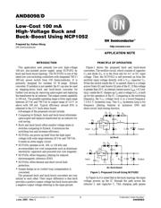
PRINCIPLE OF OPERATION
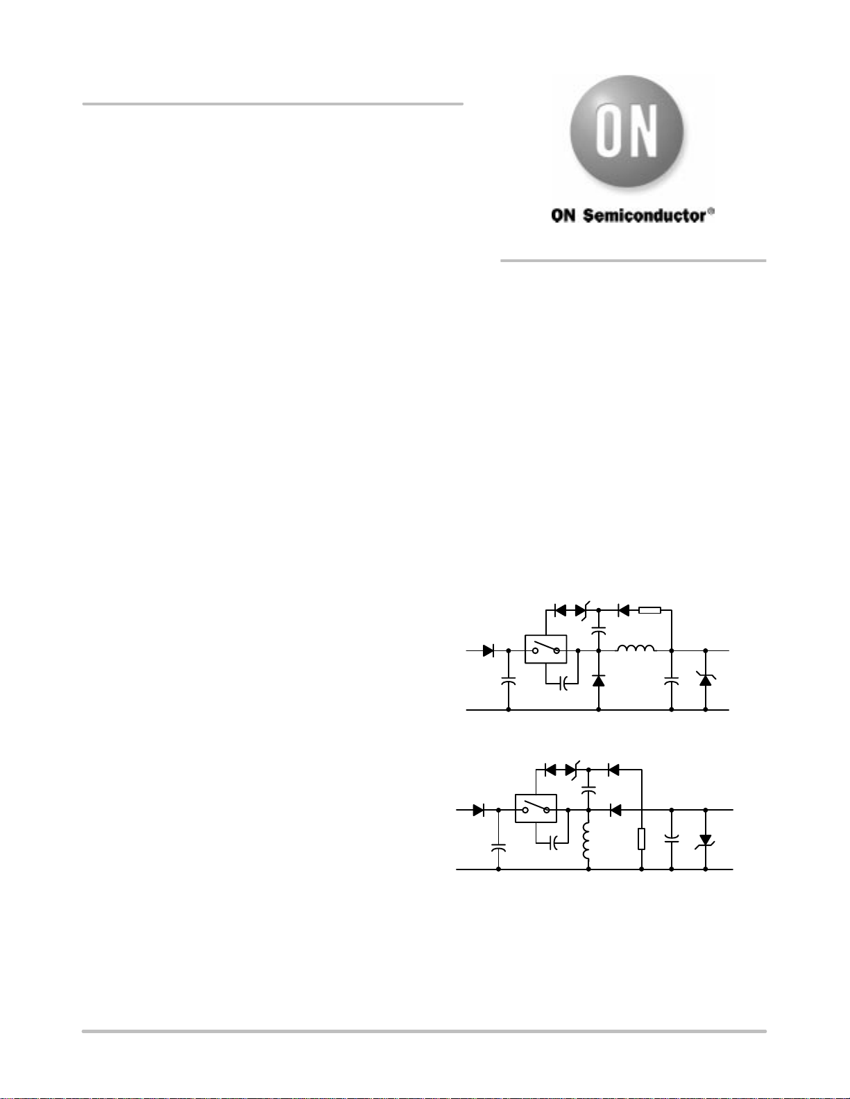
Figure 1 shows the proposed buck and buck-boost
converters. The rectifier circuit, which consists of capacitor
C
3
and diode D
3
, is in the front end for AC or DC input
voltage. Then, the NCP1052 is self-powered up from the
rectified input voltage directly with a V
CC
capacitor C
2
.
When the switch inside the IC is opened, there is a voltage
across Drain (D) and Source (S) pins of the IC. If this voltage
is greater than 20 V, an internal current source I
start
= 6.3 mA
(typ.) inside the IC charges up C
2
and a voltage in C
2
is built
up for the operation of the IC. Comparing to the switching
frequency, the V
CC
voltage level is in a lower-frequency
7.5-8.5 V hysteresis loop. This V
CC
hysteresis loop is for
frequency jittering features to minimize EMI and
short-circuit fault timing function.
Input Output
D
3
C
3
D
L
C
1
C
Z
1
C
2
V
CC
FB
DS
D
2
Z
2
D
1
R
1
(a) Buck
Input Output
D
3
C
3
D
L
C
1
C
Z
1
C
2
V
CC
FB
DS
D
2
Z
2
D
1
R
1
(b) Buck-boost
Figure 1. Proposed Circuit Using NCP1052
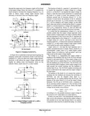
In Figure 2a it is noted that in the buck topology the input
voltage powers up the IC through the path across the
inductor L and capacitor C. This charging path passes
APPLICATION NOTE
http://onsemi.com