
下载
MW7IC2425NR1 MW7IC2425GNR1 MW7IC2425NBR1
1
RF Device Data
Freescale Semiconductor
RF Power Field Effect Transistors
N-Channel Enhancement - Mode Lateral MOSFETs
Designed primarily for CW large-signal output and driver applications at
2450 MHz. Devices are suitable for use in industrial, medical and scientific
applications.
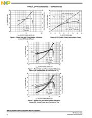
• Typical CW Performance: V
DD
= 28 Volts, I
DQ1
= 55 mA, I
DQ2
= 195 mA,
P
out
= 25 Watts CW, f = 2450 MHz
Power Gain — 27.7 dB
Power Added Efficiency — 43.8%
• Capable of Handling 10:1 VSWR, @ 28 Vdc, 2450 MHz, 25 Watts CW
Output Power
Features
• Qualified Up to a Maximum of 28 V
DD
Operation
• Integrated Quiescent Current Temperature Compensation with
Enable/Disable Function
(1)
• Integrated ESD Protection
• Excellent Thermal Stability
• 225°C Capable Plastic Package
• RoHS Compliant
• In Tape and Reel. R1 Suffix = 500 Units per 44 mm, 13 inch Reel.
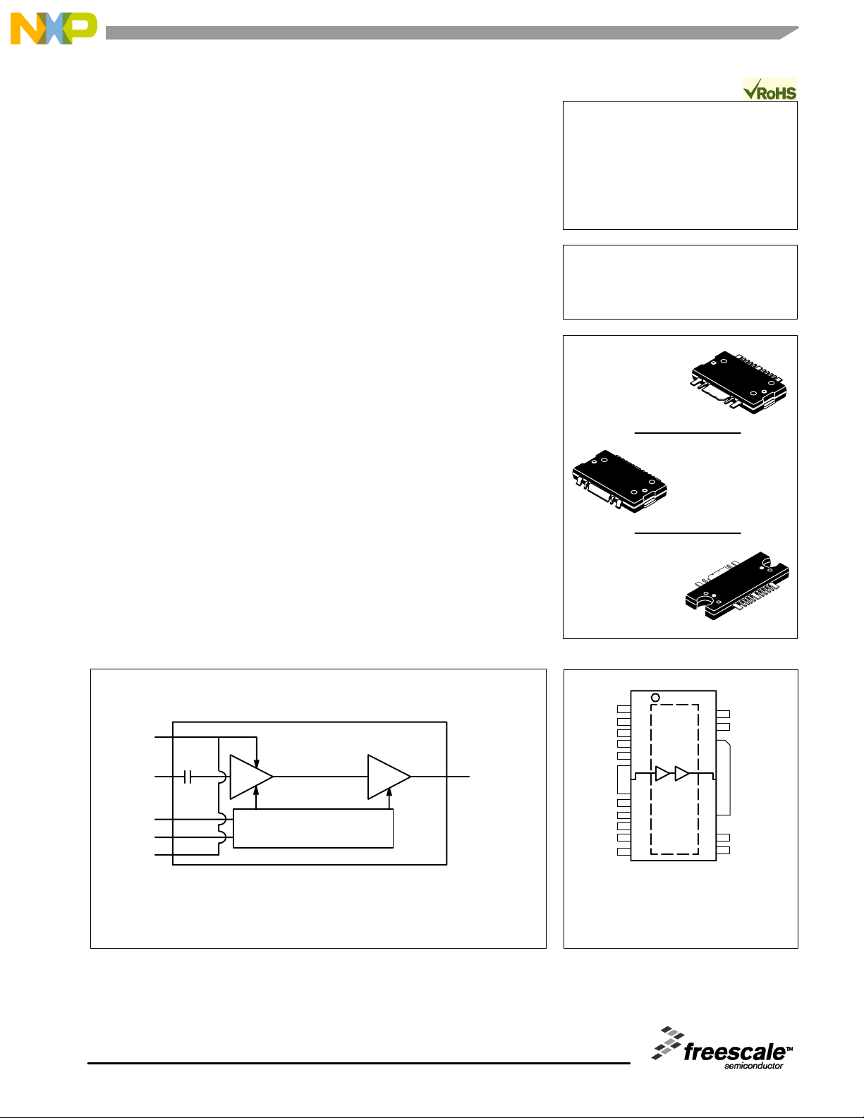
Figure 1. Functional Block Diagram
Quiescent Current
Temperature Compensation
(1)
V
DS1
RF
in
V
GS1
RF
out
/V
DS2
V
GS2
V
DS1
(Top View)
Figure 2. Pin Connections
Note: Exposed backside of the package is
the source terminal for the transistors.
GND
NC
RF
in
V
GS1
GND
RF
out
/V
DS2
GND
1
2
3
4
5
6
7
8
16
15
14
13
12
V
GS2
9
10
GND 11
V
DS1
NC
NC
NC
V
DS1
NC
NC
1. Refer to AN1977, Quiescent Current Thermal Tracking Circuit in the RF Integrated Circuit Family and to AN1987, Quiescent Current Control
for the RF Integrated Circuit Device Family. Go to http://www.freescale.com/rf. Select Documentation/Application Notes - AN1977 or AN1987.
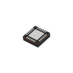
MW7IC2425NR1
MW7IC2425GNR1
MW7IC2425NBR1
2450 MHz, 25 W CW, 28 V
LATERAL N - CHANNEL
RF POWER MOSFETs
CASE 1886-01
TO-270 WB -16
PLASTIC
MW7IC2425NR1
CASE 1887-01
TO-270 WB -16 GULL
PLASTIC
MW7IC2425GNR1
CASE 1329-09
TO-272 WB -16
PLASTIC
MW7IC2425NBR1
Document Number: MW7IC2425N
Rev. 0, 3/2009
Freescale Semiconductor
Technical Data
Freescale Semiconductor, Inc., 2009. All rights reserved.