
下载
MRFE6VP5150NR1 MRFE6VP5150GNR1
1
RF Device Data
Freescale Semiconductor, Inc.
RF Power LDMOS Transistors
High Ruggedness N--Channel
Enhancement--Mode Lateral MOSFETs
These high ruggedness devices are designed for use in high VSWR
industrial (including laser and plasma exciters), broadcast (analog and digital),
aerospace and radio/land mobile applications. They are unmatched input and
output designs allow ing wide frequenc y range utiliz ation, between 1.8 and
600 MHz.
Typical Performance: V
DD
=50Vdc
Frequency
(MHz)
Signal Type
P
out
(W)
G
ps
(dB)
D
(%)
87.5–108
(1,3)
CW 179 22.5 74.6
230
(2)
CW 150 26.3 72.0
230
(2)
Pulse
(100 sec, 20%
Duty Cycle)
150 Peak 26.1 70.3
Load Mismatch/Ruggedness
Frequency
(MHz)
Signal Type VSWR
P
in
(W)
Test
Voltage
Result
98
(1)
CW
> 65:1
at all Phase
Angles
3.0
(3 dB
Overdrive)
50 No Device
Degradation
230
(2)
Pulse
(100 sec, 20%
Duty Cycle)
0.62 Peak
(3 dB
Overdrive)
1. Measured in 87.5–108 MHz broadband reference circuit.
2. Measured in 230 MHz narrowband test circuit.
3. The values shown are the m inimum measured performance numbers across the
indicated frequency range.
Features
Wide Operating Frequency Range
Extreme Ruggedness
Unmatched Input and Output Allowing Wide Frequency Range Utilization
Integrated Stability Enhancements
Low Thermal Resistance
Integrated ESD Protection Circuitry
In Tape and Reel. R1 Suffix = 500 Units, 44 mm Tape Width, 13--inch Reel.
Document Number: MRFE6VP5150N
Rev. 1, 7/2014
Freescale Semiconductor
Technical Data
1.8–600 MHz, 150 W CW, 50 V
WIDEBAND
RF POWER LDMOS TRANSISTORS
MRFE6VP5150NR1
MRFE6VP5150GNR1
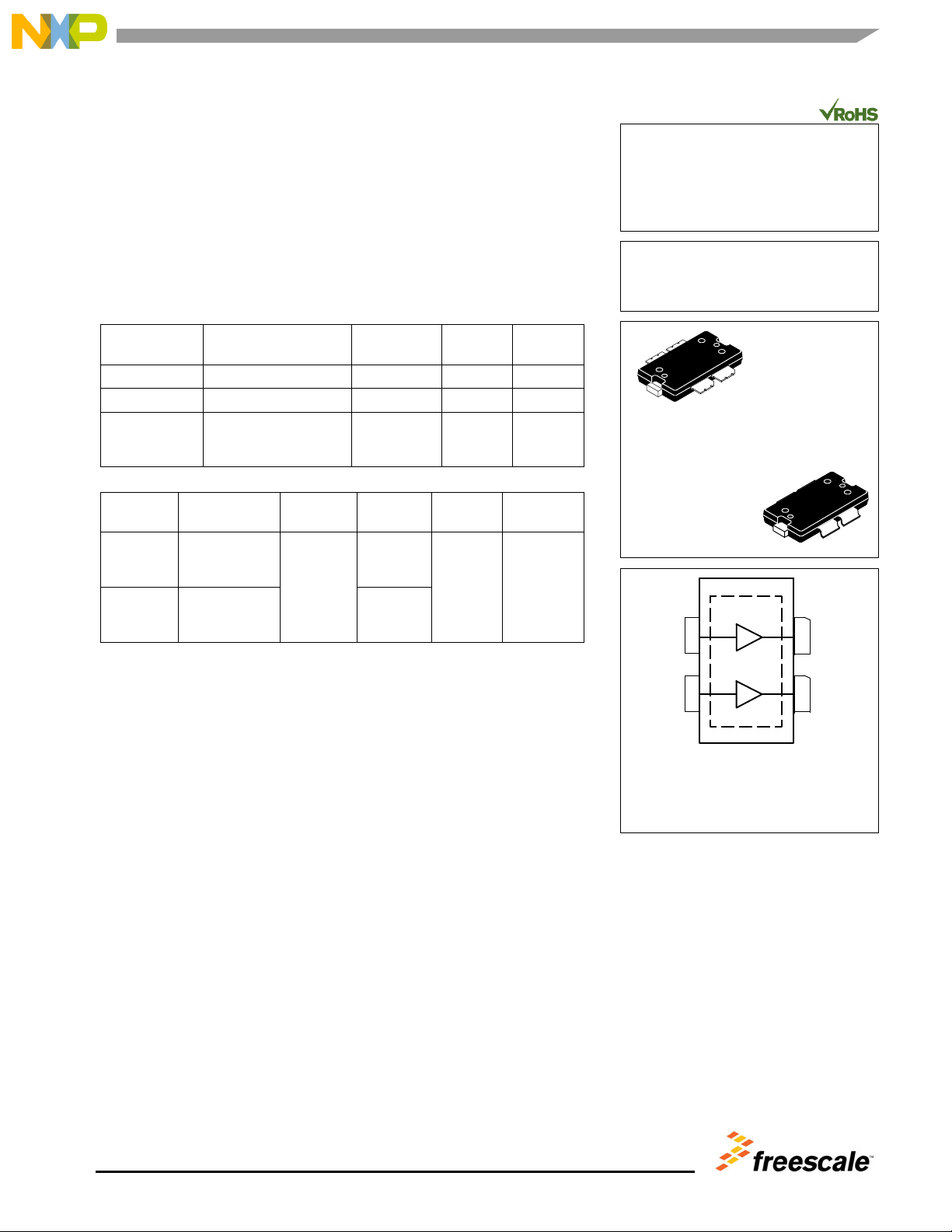
(Top View)
Drain A
32
Figure 1. Pin Connections
41
Drain B
Gate A
Note: Exposed backside of the package is
the source terminal for the transistors.
TO--270WB-- 4
PLASTIC
MRFE6VP5150NR1
TO--270WBG--4
PLASTIC
MRFE6VP5150GNR1
Gate B
Freescale Semiconductor, Inc., 2014.
A
ll rights reserved.