


下载

Application Note
MEMS Motion Handling and Assembly Guide
PURPOSE AND SCOPE
This document provides preliminary information and general guidelines for handling and assembling InvenSense Micro Electro-
Mechanical Systems (MEMS) motion sensors.
MANUFACTURING RECOMMENDATIONS
ASSEMBLY GUIDELINES AND RECOMMENDATIONS
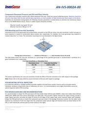
Surface Mount Packages
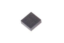
MEMS (Micro Electro-Mechanical Systems) motion sensors are generally sensitive to mechanical stress coming from the PCB.
Minimize PCB stress by following these design rules:
When using MEMS components in plastic packages, PCB mounting and assembly can cause package stress. Package stress in turn
can affect the output offset over a wide range of temperature. This stress is caused by the mismatch between the Coefficient of
Linear Thermal Expansion (CTE) of the package material and the PCB. Traces connected to pads should be as symmetric as
possible. Maximizing symmetry and balance for pad connection will help with component self-alignment and will lead to better
control of solder paste reduction after reflow.
Any material used in the surface-mount assembly process of the MEMS product should be free of restricted RoHS elements or
compounds. Pb-free solders should be used for assembly.
Offset shift may exist after the MEMS motion sensor being mounted onto the PCB board. It depends on individual applications to
decide what degree of offset shift they may tolerate. For best consistency, it is recommended to do an on-board calibration after
the accelerometer is soldered. Additional information is available upon request.
Exposed Die Pad Precautions
InvenSense products have very low active and standby current consumption. The exposed die pad is not required for heat
sinking, and should not be soldered to the PCB. Failure to adhere to this rule can induce performance changes due to package
thermo-mechanical stress. There is no electrical connection between the pad and the CMOS.
Trace Routing
Routing traces or vias under the device package is not recommended. Routed active signals may harmonically couple with the
MEMS sensor devices, compromising the sensor’s performance. To avoid harmonic coupling do not route active signals in non-
shielded signal planes directly below, or above the sensor package in cabling or adjacent PCB. Note: For best performance,
design a ground plane under the sensor to reduce PCB signal noise from the board on which the sensor is mounted. If the sensor
is stacked under an adjacent PCB board, design a ground plane directly above the sensor device to shield active signals from the
adjacent PCB board.
Component Placement
Do not place large insertion components such as keyboards or push buttons, connectors, or shielding boxes at a distance of less
than 2 mm from the MEMS motion sensor. This is to prevent mechanical stress or large thermal sink/source to the adverse of
sensor performance. Maintain generally accepted industry design practices for component placement near the device to prevent
noise coupling and thermo-mechanical stress, avoiding the neighborhood of any vibration sources like vibrator, speaker, buzzer,
and etc.
InvenSense reserves the right to change the detail
specifications as may be required to permit
improvements in the design of its products.
InvenSense Inc.
1745 Technology Drive, San Jose, CA 95110 U.S.A
+1(408) 988–7339
www.invensense.com
Document Number: AN-IVS-0002A-00
Revision: 2.5
Release Date: 11/17/2014