
下载
MMZ25332BT1
1
RF Device Data
Freescale Semiconductor, Inc.
Heterojunction Bipolar Transistor
Technology (InGaP HBT)
High Efficiency/Linearity Amplifier
The MMZ25332B is a 2--stage, high linearity InGaP HBT broadband amplifier
designed for femtocell, picocell, WLAN (802.11g/n), W--CDMA, TD--SCDMA
and LTE wireless broadband applications. It provides exceptional linearity for
LTE and W--CDMA air interfaces with an ACPR of –50 dBc at an output power
of up to 22 dBm, covering frequencies from 1500 to 2800 MHz. It operates from
a supply voltage of 3 t o 5 V. The amplifier is fully input matched, requires
minimal external matching on the output and is housed in a cost--effective,
surface mount QFN 3 × 3 package. The device offers state--of--the--art reliability,
ruggedness, temperature stability and ESD performance.
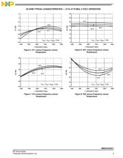
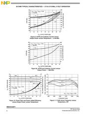
• Typical Performance: V
CC1
=V
CC2
=V
BIAS
=5Vdc,I
CQ
= 400 mA
Frequency
P
out
(dBm)
G
ps
(dB)
ACPR
(dBc)
PAE
(%)
Test Signal
2140 MHz 22 27.0 –50.0 7.0 W--CDMA
2620 MHz 21 26.0 –50.0 5.0 LTE
20 MHz
Features
• Frequency: 1500–2800 MHz
• P1dB: 33 dBm @ 2500 MHz
• Power Gain: 26.5 dB @ 2500 MHz
• OIP3: 48 dBm @ 2500 MHz
• EVM ≤ 3% @ 23.5 dBm P
out
, WLAN (802.11g)
• Active Bias Control (adjustable externally)
• Power Down Control via V
BIAS
Pin
• Class 3A HBM ESD Rating
• Single 3 to 5 V Supply
• Single--ended Power Detector
• Cost--effective 12--pin, 3 mm QFN Surface Mount Plastic Package
• In Tape and Reel. T1 Suffix = 1,000 Units, 12 mm Tape Width, 7--inch Reel.
Table 1. Typical CW Performance
(1)
Characteristic Symbol
1800
MHz
2500
MHz
2800
MHz
Unit
Small--Signal Gain (S21) G
p
27.6 26.5 25.0 dB
Input Return Loss (S11) IRL –26 –17 –16 dB
Output Return Loss
(S22)
ORL –9 –17 –16 dB
Power Output @ 1dB
Compression
P1dB 32 33 32 dBm
1. V
CC1
=V
CC2
=V
BIAS
=5Vdc,T
A
=25°C, 50 ohm system,
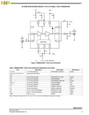
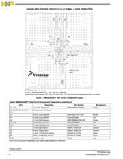
CW Application Circuit
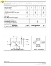
Table 2. Maximum Ratings
Rating Symbol Value Unit
Supply Voltage V
CC
6 V
Supply Current I
CC
1200 mA
RF Input Power P
in
30 dBm
Storage Temperature Range T
stg
–65 to +150 °C
Junction Temperature T
J
175 °C
Table 3. Thermal Characteristics
Characteristic Symbol Value
(2)
Unit
Thermal Resistance, Junction to Case
Case Temperature 92°C, V
CC1
=V
CC2
=V
BIAS
=5Vdc
R
θ
JC
16 °C/W
2. Refer to AN1955, Thermal Measurement Methodology of RF Power Amplifiers. Go to http://www.freescale.com/rf.
Select Documentation/Application Notes -- AN1955.
Freescale Semiconductor
Technical Data
Document Number: MMZ25332B
Rev. 2, 5/2014
1500–2800 MHz, 26.5 dB
33 dBm, 5.8 NF
InGaP HBT LINEAR AMPLIFIER
MMZ25332BT1
QFN 3 × 3
© Freescale Semiconductor, Inc., 2012, 2014. All rights reserved.
页面指南